Lamination type electronic component

a technology of electronic components and lamination, applied in the direction of impedence networks, structural fixed capacitor combinations, inductances, etc., can solve the problems of inability to change the frequency of the attenuation pole of the filter, the inductance of the coil changes, and the inability to so as to minimize the variation of electrical characteristics and prevent the change of the inductance value of the coil

Active Publication Date: 2006-02-02
MURATA MFG CO LTD
View PDF3 Cites 13 Cited by
  • Summary
  • Abstract
  • Description
  • Claims
  • Application Information

AI Technical Summary

Benefits of technology

[0011] In order to overcome the problems described above, preferred embodiments of the present invention provide a lamination type electronic component in which disposition of the conductor patterns constituting a coil is planned and, even if slight displacement is caused between the adjacent conductor patterns in the lamination direction, variations in the inductance value of the coil are prevented and variations in electrical characteristics are minimized.

Problems solved by technology

For example, in a LC filter having a capacitor contained in addition to a coil where the conductor patterns are connected in order inside a chip-type ceramic laminate, there is a problem in that the inductance of the coil changes by a change of the facing area between conductor patterns and the frequency of the attenuation pole of the filter changes.
Moreover, the lamination displacement inevitably occurs.

Method used


Image

  • Lamination type electronic component
  • Lamination type electronic component
  • Lamination type electronic component

Examples


Embodiment Construction

[0030] Hereinafter, preferred embodiments of a lamination type electronic component according to the present invention are described with reference to the attached drawings.

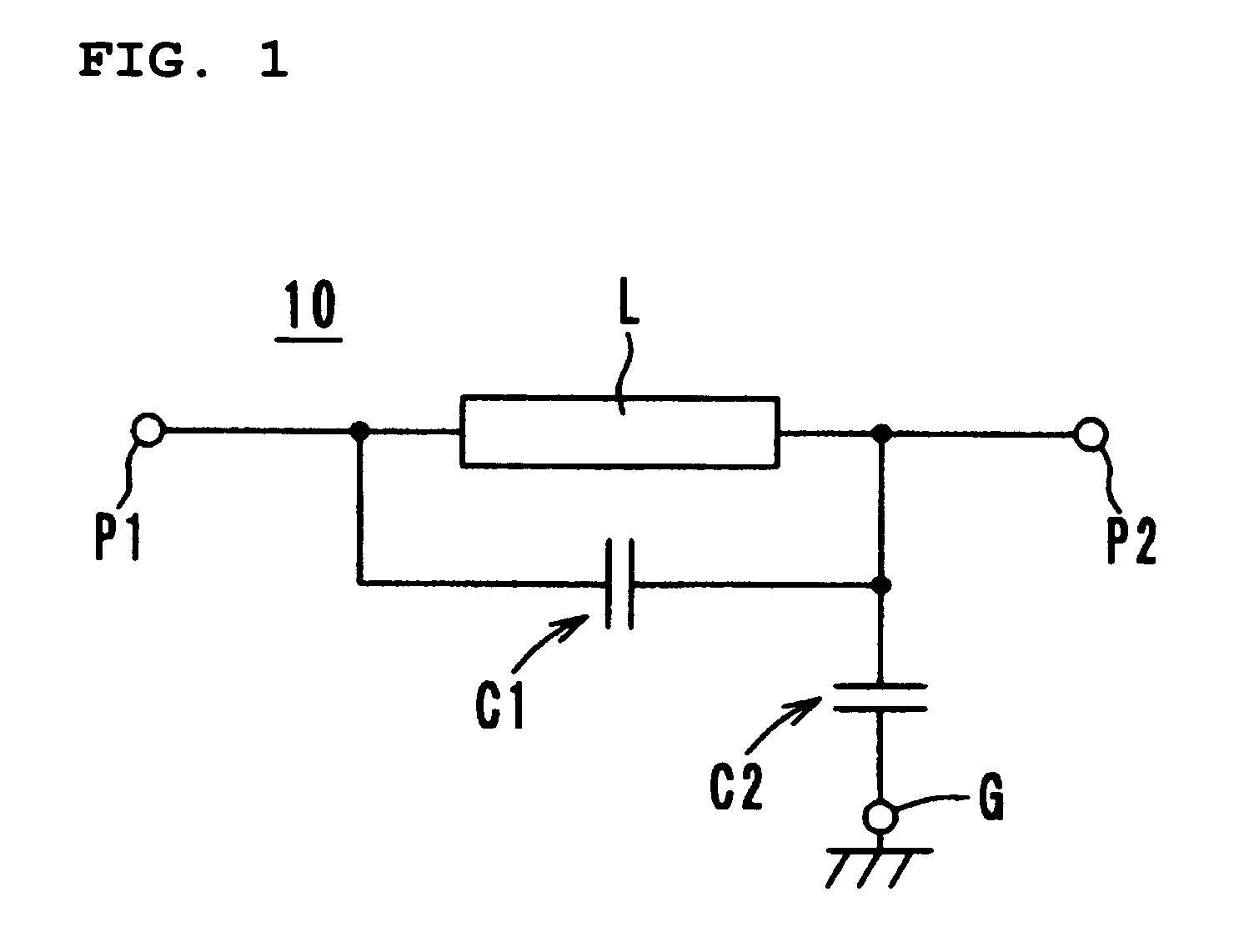
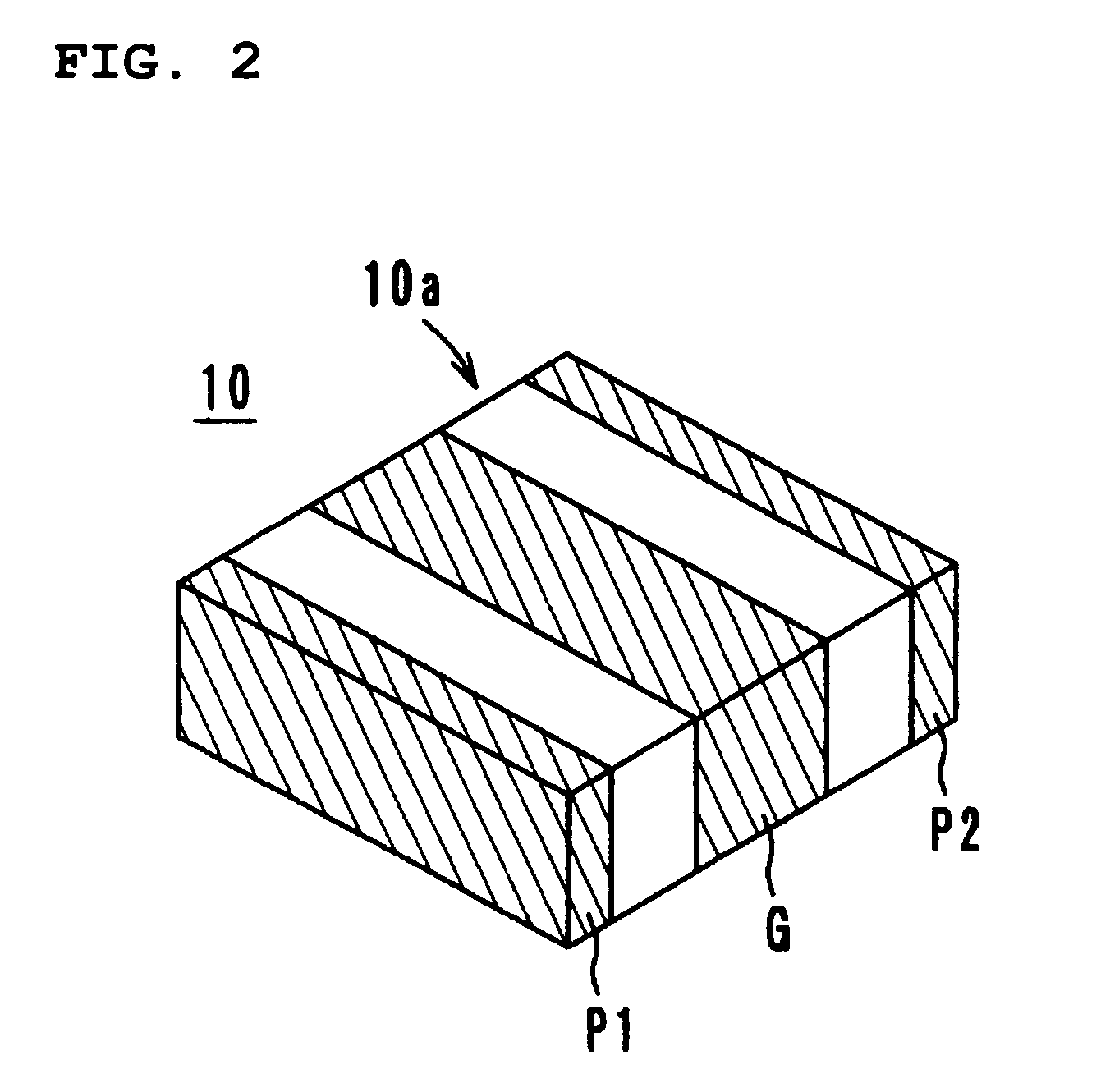
[0031] A lamination type electronic component of a preferred embodiment of the present invention is applied to an LC filter having an equivalent circuit as shown in FIG. 1, the appearance is shown in FIG. 2, and the specific structure is shown in FIG. 3.

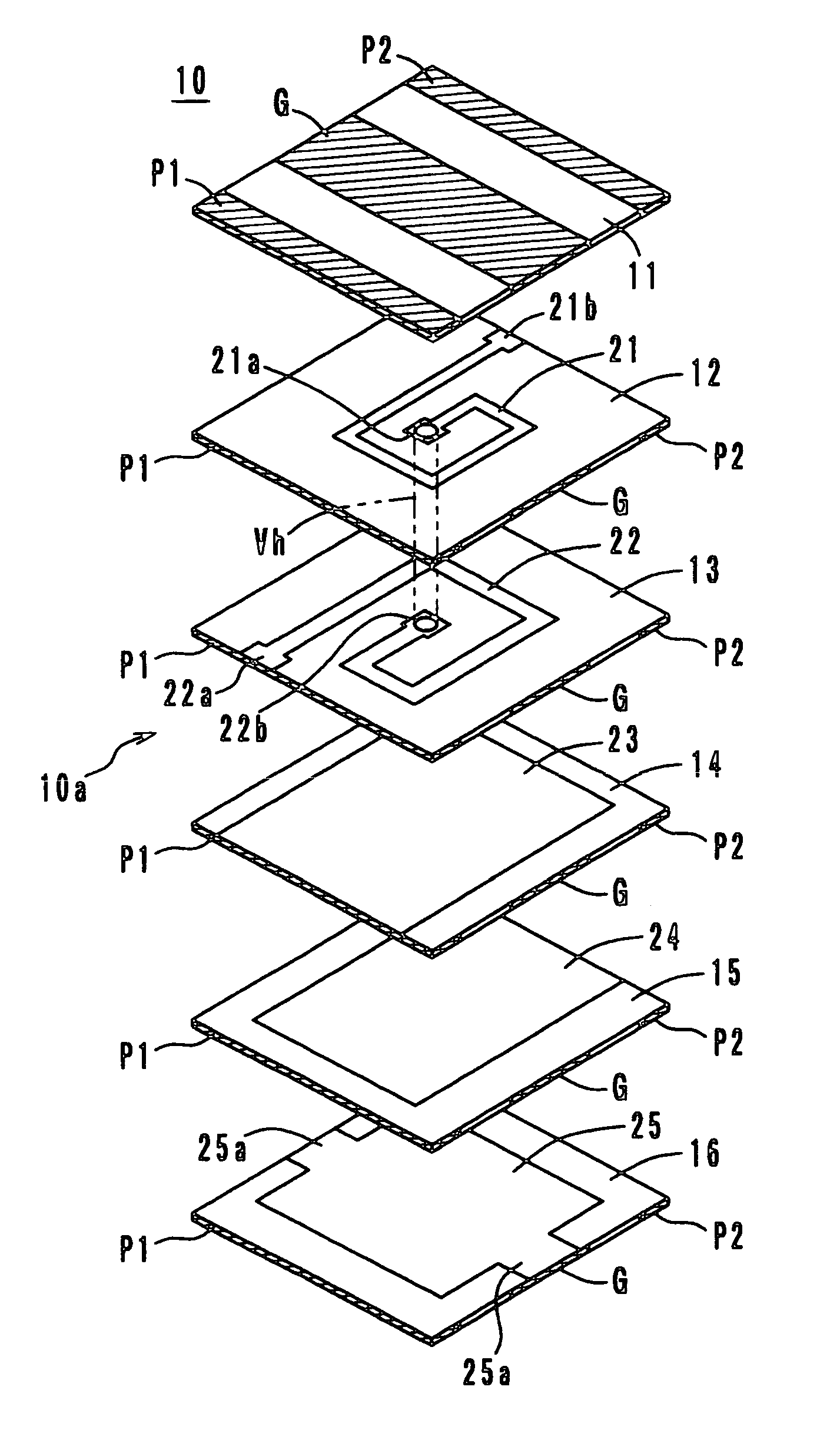
[0032] This LC filter 10 is preferably composed of a chip-like ceramic laminate 10a in which, as shown in FIG. 3, ceramic insulating layers 11 to 16 made of ceramic material are laminated. Each of the ceramic insulating layers 11 to 16 is preferably made up of a ceramic green sheet formed by a doctor blade method, a pull-up method, etc., using a ceramic material and the ceramic laminate 10a is formed by using the ceramic green sheets laminated and attached together by pressure and then fired.

[0033] As shown in FIG. 2, an input terminal P1 of the LC filter 10 is...


PUM


Abstract

A lamination type electronic component includes spiral conductor patterns which are substantially quadrilateral and are electrically connected to each other through a via hole formed in a ceramic insulating layer so as to constitute a coil. The conductor patterns are arranged so that the center in the width direction of the sides extending in the Y-axis direction of the one conductor pattern may be positioned at the inside edges of the sides extending in the Y-axis direction of the other conductor pattern.

Description

BACKGROUND OF THE INVENTION [0001] 1. Field of the Invention [0002] The present invention relates a lamination type electronic component and more particularly, to a lamination type electronic component of an LC filter having a coil disposed inside a laminate made up of laminated insulating layers of ceramic, etc. [0003] 2. Description of the Related Art [0004] Up to now, for example, a laminated inductor disclosed in Japanese Unexamined Patent Application Publication No. 2002-64016 is known among such lamination type electronic components. In the laminated inductor, ceramic insulating layers and conductor patterns are alternately laminated, the conductor patterns are stacked one upon another in the lamination direction of the ceramic insulation layers by connecting the end portion of each conductor pattern in order, and a coil in which the direction of the coil axis is in the lamination direction of the ceramic insulating layers is formed within a chip-type ceramic laminate. [0005] ...

Claims


Application Information

Patent Timeline
Patent Type & Authority Applications(United States)
IPC IPC(8): H03H7/00
CPCH01F17/0013H01F2017/0026H01G4/40H03H2001/0092H03H7/1766H03H2001/0085H03H7/0115
Inventor ASAKAWA, KEIJI
Owner MURATA MFG CO LTD
Why Eureka
Try Eureka