Liquid crystal display device and manufacturing method thereof

a technology of liquid crystal display and manufacturing method, which is applied in the direction of sewer systems, ways, constructions, etc., can solve the problems of undesired organic layer formation, degradation of image quality, and increase in both the thickness of lcd and its production cost, so as to prevent an electrical short

Active Publication Date: 2006-02-02
LG DISPLAY CO LTD
View PDF1 Cites 42 Cited by
  • Summary
  • Abstract
  • Description
  • Claims
  • Application Information

AI Technical Summary

Benefits of technology

[0033] An advantage of the present invention is to provide a liquid crystal display device and a manufacturing method thereof, in which an array unit and a color filter layer is formed on one substrate, a black matrix is also formed on the substrate, and a pattern spacer is disposed at an ESD circuit at the outer portion thereof, thereby protecting the ESD circuit and preventing an electrical short due to an electrostatic discharge.
[0034] Additional advantages and features of the invention will be set forth in part in the description which follows and in part will become apparent to those having ordinary skill in the art upon examination of the following or may be learned from practice of the invention. The objectives and other advantages of the invention may be realized and attained by the structure particularly pointed out in the written description and claims hereof as well as the appended drawings.
[0035] To achieve these and other advantages and in accordance with the purpose of the invention, as embodied and broadly described herein, there is provided an LCD having a liquid crystal panel including an active region serving as a display region and an outer region serving as a non-display region, the LCD including: a first substrate including an array unit and a color filter formed in the active region; an ESD circuit formed in the outer region; a pattern spacer formed on the ESD; a second substrate facing the first substrate; and a sealant for attaching the first and second substrates together.
[0036] In another aspect of the present invention, there is provided a method for manufacturing an LCD, the method including: forming an array unit, a color filter and a black matrix in a display region on a first substrate and forming an ESD circuit and an outer black matrix in a non-display region; forming a pattern spacer in the display region and forming a pattern spacer on a partial surface or an entire surface of the ESD circuit; attaching the first substrate and a second substrate facing the first substrate together using a sealant; and forming a liquid crystal layer between the first and second substrates.
[0037] In a further another aspect of the present invention, there is provided an LCD having a liquid crystal panel includin

Problems solved by technology

In the COT-type LCD 190, there occurs light leakage at the boundary region D between the non-display region E and the display region C, resulting in the degradation of an image quality.
The second overcoat layer formed on the black matrix causes an undesirable increase in both the thickness of the LCD and its production cost.
When th

Method used


Image

  • Liquid crystal display device and manufacturing method thereof
  • Liquid crystal display device and manufacturing method thereof
  • Liquid crystal display device and manufacturing method thereof

Examples


first embodiment

[0051]FIG. 3 is a sectional view of a COT-type LCD according to the present invention.

[0052] Referring to FIG. 3, the COT-type LCD includes a first substrate 200. A gate electrode 212 is formed on the first substrate 200 and a gate insulating layer 232a is formed on the gate electrode 212.

[0053] A gate pad is formed at an end of a gate line connected to the gate electrode 212.

[0054] An active layer 214 and an ohmic contact layer 215 are sequentially stacked on the gate insulating layer 232a corresponding to the gate electrode 212. Source and drain electrodes 216 and 218 are formed on the ohmic contact layer 215 to contact with the ohmic contact layer 215 and to be spaced part from each other by a predetermined distance.

[0055] A first overcoat layer 232b for protecting the active layer 214 is formed of inorganic material on an entire surface of the first substrate 200 on which the source and drain electrodes 216 and 218 have been formed.

[0056] A color filter 220 contacting with t...

second embodiment

[0076]FIG. 4 is a sectional view of a COT-type LCD according to the present invention.

[0077] In this embodiment, a detailed description about the same elements as in FIG. 3 will be omitted for simplicity.

[0078] Referring to FIG. 4, an ESD circuit is formed at an outer portion of the panel and a pattern spacer is formed on the ESD circuit.

[0079] Here, the ESD circuit is formed inwardly from the sealant 294.

[0080] In addition, the ESD circuit may be formed between the sealant 294 and a black matrix 222 formed at the outer portion.

third embodiment

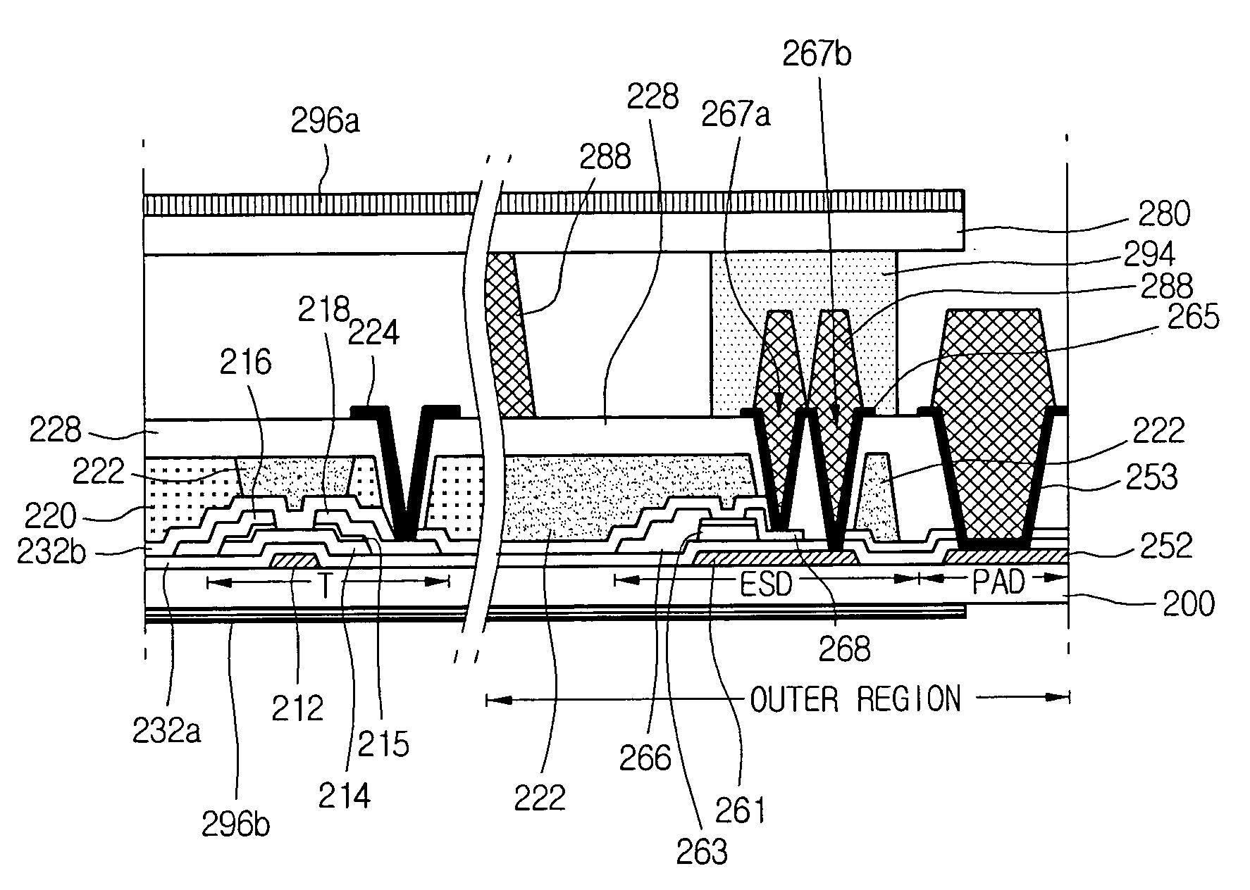
[0081]FIG. 5 is a sectional view of a COT-type LCD according to the present invention.

[0082] In this embodiment, a detailed description about the same elements as in FIG. 3 will be omitted for simplicity.

[0083] Referring to FIG. 5, an ESD circuit is formed at an outer portion of the panel and a pattern spacer 288 is formed on the ESD circuit.

[0084] Here, the ESD circuit is formed outwardly from a sealant 264.

[0085] In addition, the ESD circuit may be formed between the sealant 264 and a gate pad 252.

[0086] When the ESD circuit is formed outwardly from the sealant 264 and the pattern spacer 288 is formed on the ESD circuit, the electro-chemical corrosion of the ESD circuit can be prevented.

[0087] The LCD described in these embodiments is manufactured through a 5-mask process.

[0088] The abovementioned structure can be similarly applied to a TOC-type LCD.

[0089] Also, the abovementioned structure can be similarly applied to an LCD manufactured through a 4-mask process.

[0090] Fur...


PUM


Abstract

Provided is an LCD having a liquid crystal panel including an active region serving as a display region and an outer region serving as a non-display region. The LCD includes a first substrate including an array unit and a color filter formed in the active region, an ESD (electrostatic discharge) circuit formed in the outer region, a pattern spacer formed on the ESD, a second substrate facing the first substrate, and a sealant for attaching the first and second substrates together.

Description

[0001] This application claims the benefit of Korean Patent Application Nos. 2004-60527, filed Jul. 30, 2004, and 2005-14261, filed Feb. 21, 2005, which are hereby incorporated by reference for all purposes as if fully set forth herein. BACKGROUND OF THE INVENTION [0002] 1. Field of the Invention [0003] The present invention relates to a liquid crystal display device, and more particularly, to a liquid crystal display device preventing damage in an electrostatic discharge circuit and a manufacturing method thereof. [0004] 2. Discussion of the Related Art [0005] The growth of the information technology and consumer electronics industries has driven the need for a next generation display device capable of processing and displaying the large capacity image information increases gradually. [0006] Such next generation display devices are required to be lighter, thinner, shorter and smaller characteristics, a high luminance, a large-sized screen, low power consumption and a low price. Exa...

Claims


Application Information

Patent Timeline
IPC IPC(8): G02F1/1333
CPCG02F1/136204G02F2001/136222G02F1/136209G02F1/136222E01C11/227E03F3/046
Inventor PARK, SEUNG RYULL
Owner LG DISPLAY CO LTD
Why Eureka
Try Eureka