Method for fabricating semiconductor device using amorphous carbon layer as sacrificial hard mask

a technology of amorphous carbon layer and a semiconductor device, which is applied in the direction of semiconductor/solid-state device manufacturing, electrical equipment, basic electric elements, etc., can solve the problems of time delay, difficult to develop a material for the arf photoresist, and difficult to obtain a pattern below the size of 0.1 m, so as to reduce the pattern deformation and increase the selectivity of the etching hard mask

Active Publication Date: 2006-02-02
SK HYNIX INC
View PDF4 Cites 232 Cited by
  • Summary
  • Abstract
  • Description
  • Claims
  • Application Information

AI Technical Summary

Benefits of technology

[0025] It is, therefore, an object of the present invention to provide a method for fabricating a semiconduct

Problems solved by technology

However, this photolithography is disadvantageous in an incidence of a time delay at an initial stage of the photolithography and dependent on properties of an employed material.
Even if various photolithography techniques are combined to improve resolution of the above mentioned DUV photolithography, it is very difficult to obtain a pattern below the size of 0.1 μm.
Especially, it is difficult to develop a material for the ArF photoresist because it is not allowed to use a benzene ring which is used for the KrF and i-line photoresist to secure a tolerance to a dry etching process.
However, when the benzene ring is used for the ArF photoresist, absorption of the benzene ring is large at a wavelength of 193 nm of the ArF laser, resulting in a

Method used


Image

  • Method for fabricating semiconductor device using amorphous carbon layer as sacrificial hard mask
  • Method for fabricating semiconductor device using amorphous carbon layer as sacrificial hard mask
  • Method for fabricating semiconductor device using amorphous carbon layer as sacrificial hard mask

Examples


first embodiment

[0060]FIGS. 8A to 8F are cross-sectional views illustrating a method for forming a pattern in a semiconductor device through performing a F2 or ArF photolithography in accordance with the present invention.

[0061] Among various types of line-type patterns, the case of forming bit lines is exemplified in the first embodiment of the present invention. However, this embodied line-type pattern formation is also applicable to other various types of patterns for forming gate structures, storage node contacts, metal lines and so on.

[0062] Also, in addition to the line-type, an island type and a donut-shaped type as like the shape of a storage node contact can also be applicable. Furthermore, although the above line-type pattern is based on a conductive layer, an insulation layer can also be used. Additionally, the line-type pattern illustrated in the first embodiment is a positive pattern.

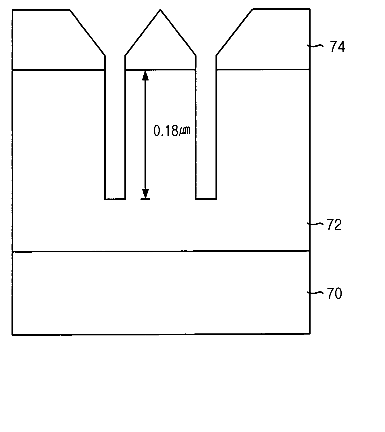
[0063] Referring to FIG. 8A, a conductive layer 61A is formed as an etch target layer on a substrate ...

fourth embodiment

[0088] In the fourth embodiment, the anti-reflective coating layer 65A uses SiON, which is an inorganic material, and the amorphous carbon layer 63A is disposed beneath the anti-reflective coating layer 65A. Also, the anti-reflective coating layer 65A is intended to provide the originally assigned functions and an additional function as a sacrificial hard mask. Thus, the anti-reflective coating layer 65A is formed in a thickness ranging from approximately 200 Å to approximately 1,000 Å to realize the etching process even with the thinly formed photoresist pattern 66A.

[0089] Also, the anti-reflective coating layer 65A and the sacrificial hard mask layer 64A can be substituted with a material selected from a group consisting of oxide, nitride, oxynitride and a combination thereof. The amorphous carbon layer 63A is formed in a thickness greater than at least approximately 1,000 Å, typically, greater than approximately 2,000 Å for the purpose of securing an intended level of etch select...

fifth embodiment

[0090]FIGS. 12A to 12D are cross-sectional views illustrating a method for forming a pattern in a semiconductor device by employing a F2 or ArF photolithography process in accordance with the present invention.

[0091] In the fifth embodiment, the exemplified pattern is for forming a contact hole. More specifically, this contact hole pattern can be applicable to a metal line contact, a contact between one of a bit line and a storage node of a capacitor and an impurity junction such as a source / drain and a contact pad. Also, the contact hole pattern can be applicable to a process for forming a trench for device isolation in which an etch target is an insulation layer and to a process for etching an etch target based on a conductive material, e.g., a polysilicon layer, to open a channel region of a thin film transistor. That is, these pattern formation processes are negative type of patterns.

[0092] Referring to FIG. 12A, an insulation layer 101 is formed as an etch target layer on a su...


PUM


Abstract

Disclosed is a method for fabricating a semiconductor device by using an amorphous carbon layer as a sacrificial hard mask. The method includes the steps of: forming an amorphous carbon layer on an etch target layer; forming a photoresist pattern on the amorphous carbon layer; etching the amorphous carbon layer by using the photoresist pattern to form a sacrificial hard mask; and etching the etch target layer by using the sacrificial hard mask to form a predetermined pattern.

Description

FIELD OF THE INVENTION [0001] The present invention relates to a method for fabricating a semiconductor device; and, more particularly, to a method for forming a pattern in a semiconductor device through an advanced photolithography process compared with a typical ArF or F2 photolithography. DESCRIPTION OF RELATED ARTS [0002] Photolithography is one advanced fine manufacturing process that has made a contribution to a current astonishing progression in semiconductor devices. Especially, an improvement on resolution of the photolithography is a critical factor for advancing an integration scale of semiconductor devices. [0003] As known, photolithography includes a process for forming a photoresist pattern and a process for forming desired patterns like line patterns, for instance, contact holes and gate structures, by etching an etch target with use of the photoresist pattern as an etch mask. Herein, the photoresist pattern is formed through sequential processes including a process f...

Claims


Application Information

Patent Timeline
IPC IPC(8): H01L21/469
CPCH01L21/0332H01L21/32139H01L21/3146H01L21/02115H01L21/306
Inventor KIM, KWANG-OKCHO, YUN-SEOK
Owner SK HYNIX INC
Why Eureka
Try Eureka