GaN LED structure with p-type contacting layer grown at low-temperature and having low resistivity

a technology of led structure and contacting layer, which is applied in the direction of basic electric elements, electrical equipment, and semiconductor devices, can solve the problems of increased energy consumption and inability of the epitaxy to keep the regular structure formed, and achieves the effects of reducing energy gap, reducing resistivity, and improving reliability

Active Publication Date: 2006-02-09
FORMOSA EPITAXY INCORPORATION +1
View PDF4 Cites 9 Cited by
  • Summary
  • Abstract
  • Description
  • Claims
  • Application Information

AI Technical Summary

Benefits of technology

[0003] The present invention has been made to overcome the above-mentioned drawback of conventional GaN MQW LED structures that need a high temperature to grow a p-type contacting layer. The primary object of the present invention is to provide a GaN MQW LED structure with a low resistive p-type contacting layer that is made of In1-yGayN codoped with Mg and Al, and can be grown at low temperature. The resistivity of the p-type contact layer of the present invention is lower than that of the conventional p-type contactin...

Problems solved by technology

During the manufacturing, it is found that the contacting layer grown at high temperature will affect the epitaxial characteristics of the active layer grown at low temperature in the previous step, so that the epitaxy will not keep...

Method used


Image

  • GaN LED structure with p-type contacting layer grown at low-temperature and having low resistivity
  • GaN LED structure with p-type contacting layer grown at low-temperature and having low resistivity
  • GaN LED structure with p-type contacting layer grown at low-temperature and having low resistivity

Examples


first embodiment

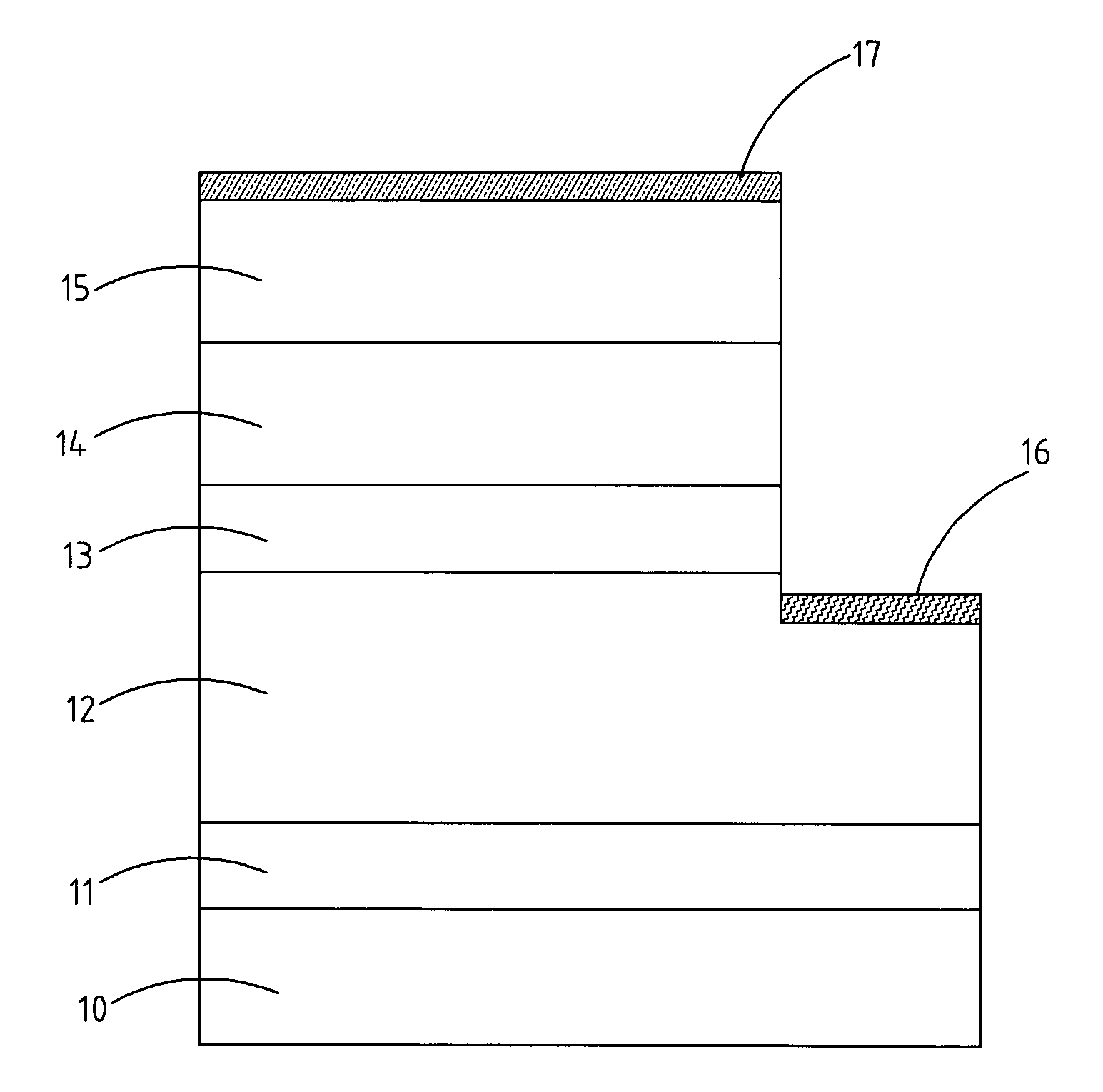
[0012]FIG. 1 shows the present invention of a GaN LED structure having a p-type contacting layer grown at low temperature and having low resistivity. The embodiment includes a substrate 10, a buffer layer 11, an n-type GaN layer 12, an active layer 13, a p-type shielding layer 14, and a p-type contacting layer 15. Substrate 10 can be made of sapphire (including C-Plane, R-Plane and A-Plane), SiC (6H—SiC or 4H—SiC), Si, ZnO, GaAs, and MgAl2O4. It can also be made of single crystal oxide having the lattice constant close tot hat of the N-compound semiconductor. But, in general, it is made of sapphire and SiC. Buffer layer 11 is located on top of substrate 10, and is made of Al1-x-yGaxInyN , where 0≦x<1, 0≦y<1 and x+y≦1.

[0013] Located on top of buffer layer 11 is n-type GaN layer 12. Active layer 13, which is located on top n-type GaN layer 12, is made of Al1-x-yGaxInyN. Located on top of the active layer 13 is a p-type shielding layer 14, which is made of Mg-doped p-type Al1-xInxN, wh...

second embodiment

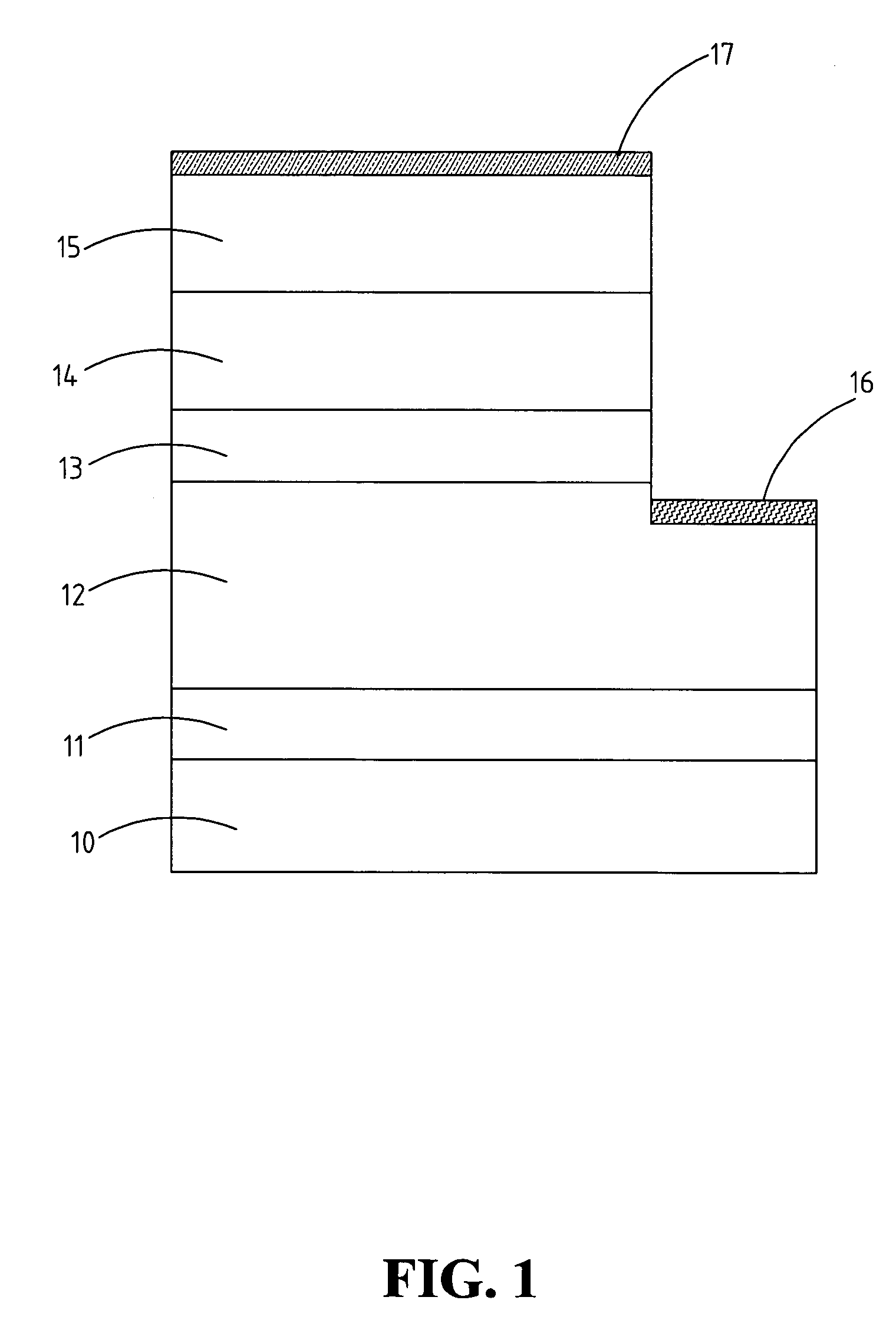
[0015]FIG. 2 shows the present invention of a GaN LED structure having a p-type contacting layer grown at low temperature and having low resistivity. The embodiment includes a substrate 20, a buffer layer 21, an n-type GaN layer 22, an active layer 23, a p-type shielding layer 24, and a p-type contacting layer 25. Substrate 20 can be made of sapphire (including C-Plane, R-Plane and A-Plane), SiC (6H—SiC or 4H—SiC), Si, ZnO, GaAs, and MgAl2O4. It can also be made of single crystal oxide having the lattice constant close tot hat of the N-compound semiconductor. But, in general, it is made of sapphire and SiC. Buffer layer 21 is located on top of substrate 20, and is made of Al1-x-yGaxInyN, where 0≦X<1, 0≦Y<1, and X+Y≦1.

[0016] Located on top of buffer layer 21 is n-type GaN layer 22. Active layer 23, which is located on top n-type GaN layer 22, is made of Al1-x-yGaxInyN Located on top of active layer 23 is p-type shielding layer 24, which is made of Mg—Ga-codoped p-type Al1-xInxN, wher...

third embodiment

[0018]FIG. 3 shows the present invention of a GaN LED structure having a p-type contacting layer grown at low temperature and having low resistivity. The embodiment includes a substrate 30, a buffer layer 31, an n-type GaN layer 32, an active layer 33, a double shielding layer 34, and a p-type contacting layer 35. Substrate 30 can be made of sapphire (including C-Plane, R-Plane and A-Plane), SiC (6H—SiC or 4H—SiC), Si, ZnO, GaAs, and MgAl2O4. It can also be made of single crystal oxide having the lattice constant close tot hat of the N-compound semiconductor. But, in general, it is made of sapphire and SiC. Buffer layer 31 is located on top of substrate 30, and is made of Al1-x-yGaxInyN, where 0≦X<1, 0≦Y<1, and X+Y≦1.

[0019] Located on top of buffer layer 31 is n-type GaN layer 32. Active layer 33, which is located on top n-type GaN layer 32, is made of Al1-x-yGaxInyN. Located on top of active layer 33 is double shielding layer 34,which further includes a first shielding layer 340, a...


PUM


Abstract

Disclosed is a GaN LED structure with a p-type contacting layer using Al—Mg-codoped In1-yGayN grown at low temperature, and having low resistivity. The LED structure comprises, from the bottom to top, a substrate, a buffer layer, an n-type GaN layer, an active layer, a p-type shielding layer, and a p-type contacting layer. In this invention, Mg and Al are used to co-dope the In1-yGayN to grow a low resistive p-type contacting layer at low temperature. Because of the Al—Mg-codoped, the light absorption problem of the p-type In1-yGayN layer is improved. The product, not only has the advantage of convenience of the p-type contacting layer for being manufactured at low temperature, but also shows good electrical characteristics and lowers the operating voltage of the entire element so that the energy consumption during operation is reduced and the yield rate is increased.

Description

FIELD OF THE INVENTION [0001] The present invention generally relates to a structure for InGaN / GaN multiquantum well (MQW) light emitting diodes (LED), and more specifically to an LED structure with a p-type contacting layer made with Al—Mg-codoped In1-yGayN grown at low temperature and having low resistivity. BACKGROUND OF THE INVENTION [0002] Conventional multiquantum well (MQW) In1-yGayN / GaN light emitting diodes (LED) use a p-type GaN grown at high temperature as a contacting layer. The contacting layer is usually grown on top of the active (light-emitting) layer. During the manufacturing, it is found that the contacting layer grown at high temperature will affect the epitaxial characteristics of the active layer grown at low temperature in the previous step, so that the epitaxy will not keep the regular structure formed during its growth. The result of this effect is that the LED is either dysfunctional, or has poor electrical characteristics, such as having higher operating vo...

Claims


Application Information

Patent Timeline
IPC IPC(8): H01L33/00H01L33/32H01L33/40
CPCH01L33/40H01L33/32
Inventor WU, LIANG-WENTU, RU-CHINYU, CHENG-TSANGWEN, TZU-CHICHIEN, FEN-REN
Owner FORMOSA EPITAXY INCORPORATION
Why Eureka
Try Eureka