Method for processing base

a technology of processing base and base plate, which is applied in the direction of semiconductor devices, semiconductor/solid-state device details, electrical apparatus, etc., can solve the problems of uneven surface, inability to grind, and uneven surface, etc., and achieve low cost, low damage, and high reliability

Inactive Publication Date: 2006-02-09
FUJITSU LTD
View PDF0 Cites 39 Cited by
  • Summary
  • Abstract
  • Description
  • Claims
  • Application Information

AI Technical Summary

Benefits of technology

[0037] An object of the present invention is to solve the above problems and provide a joined base which is low in cost, has an even and smooth height, enables forming of metal te...

Problems solved by technology

When the above-described conventional arts are applied to formation of metal terminals of an electronic component such as an LSI and a mounting step thereof, following problems arise.
If an object to be ground is a soft material such as a resin, there arises a problem (burn) such that dust from the grinding adheres to a surface of a grinding disk and the grinding becomes impossible.
There also arises another problem such that a resin or a metal being a base material of the grinding disk contaminates the surface of the resin being the object to be ground.
In such a case of planarization by the polishing, there arises a prob...

Method used


Image

  • Method for processing base
  • Method for processing base
  • Method for processing base

Examples


first embodiment

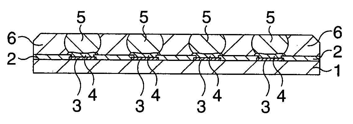
[0096]FIG. 1 is a schematic sectional view showing a method for manufacturing a semiconductor device according to a first embodiment step by step.

[0097] Here, a first base is a semiconductor chip which is diced from a semiconductor wafer and on a principal surface of which electrode terminals are disposed, and a second base is a circuit board on which the semiconductor chip is to be flip-chip mounted. Now, a case that the semiconductor chip is mounted on the circuit board is described. The circuit board includes an insulating substrate formed of glass epoxy and the like, and a conductive layer formed on the surface and / or inside thereof. On its mounting surface for the semiconductor chip, there are disposed electrode terminals corresponding to electrode terminals of the semiconductor chip to be mounted.

[0098] In the present embodiment, after a surface, i.e., a mounted surface, of the semiconductor chip is planarized by cutting, the electrode terminals of the semiconductor chip and...

second embodiment

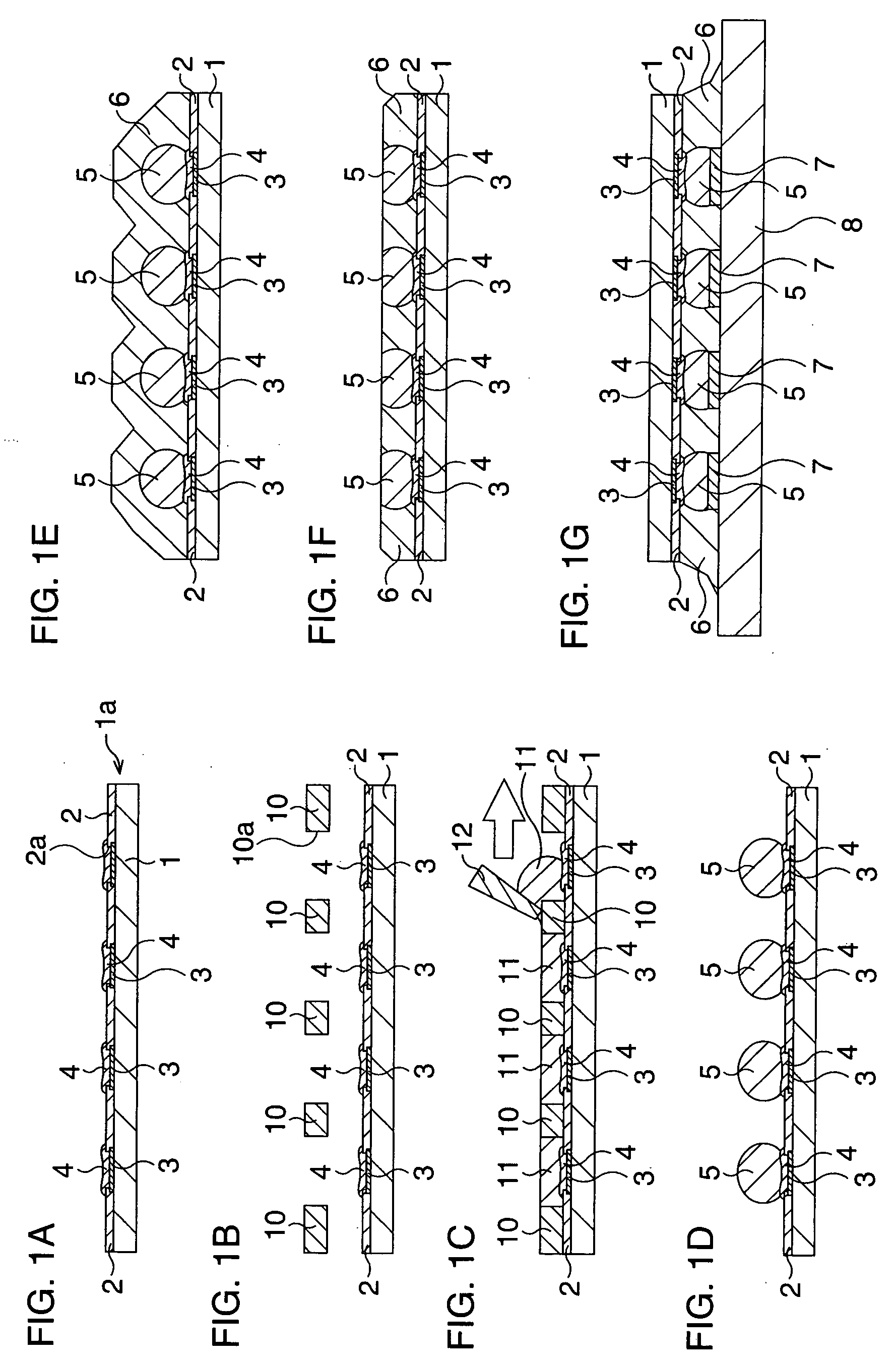
[0132]FIG. 3 is a schematic sectional view showing a method for manufacturing a semiconductor device according to a second embodiment step by step. For description convenience, wordings such as “second temperature” are used in descriptions below, but they are unrelated to the “second temperature” and the like in the above first embodiment.

[0133] Here, a first base is a semiconductor chip which is diced from a semiconductor wafer and on a principal surface of which electrode terminals are disposed, and a second base is a circuit board on which the semiconductor chip is to be flip-chip mounted. Now, a case that the semiconductor chip is mounted on the circuit board is described. The circuit board includes an insulating substrate formed of glass epoxy and the like, and a conductive layer formed on the surface and / or inside thereof. On its mounting surface for the semiconductor chip, there is disposed electrode terminals corresponding to the electrode terminals of the semiconductor chi...

third embodiment

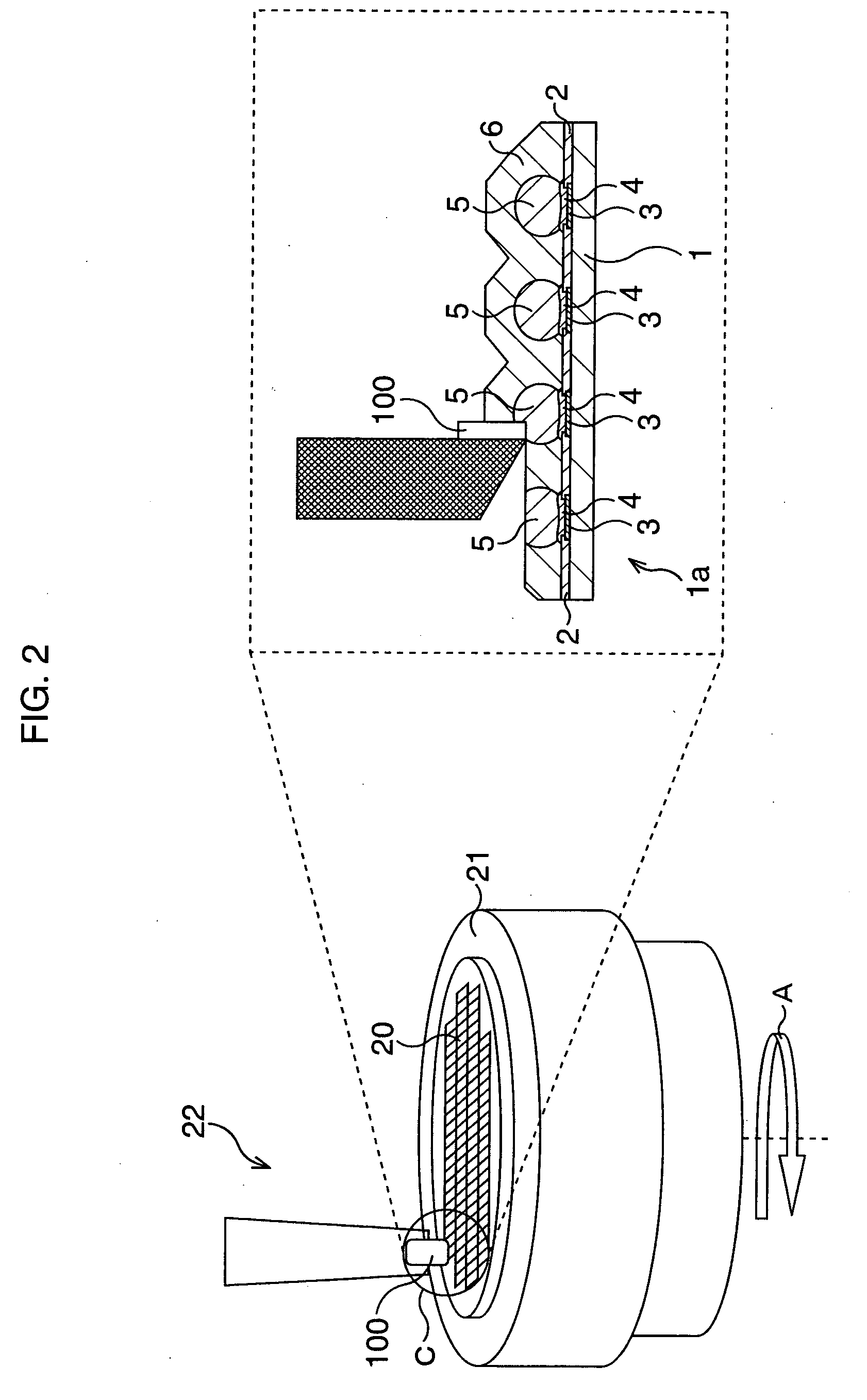
[0153]FIG. 4 is a schematic sectional view showing a method for manufacturing a semiconductor device according to a third embodiment step by step. For description convenience, wordings such as “second temperature” are used in descriptions below, but they are unrelated to the “second temperature” and the like in the first and the second embodiments described above.

[0154] Here, a first base is a semiconductor chip which is diced from a semiconductor wafer and on a principal surface of which electrode terminals are disposed, and a second base is a circuit board on which the semiconductor chip is to be flip-chip mounted. Now, a case that the semiconductor chip is mounted on the circuit board is described. The circuit board includes an insulating substrate formed of glass epoxy and the like, and a conductive layer formed on the surface and / or inside thereof. On its mounting surface for the semiconductor chip, there are disposed electrode terminals corresponding to the electrode terminal...


PUM


Abstract

Electrodes and an insulating film are both formed of materials which have characteristics that they are solid and do not exhibit adhesiveness at a room temperature, exhibit adhesiveness at and above a first temperature higher than this, and are cured at and above a second temperature higher than this. Planarication processing is carried out by performing cutting with a hard cutting tool made of diamond and the like so that surfaces film the electrodes and a surface of the insulating film become continuously planar.

Description

CROSS-REFERENCE TO RELATED APPLICATIONS [0001] This application is based upon and claims the benefit of priority from the prior Japanese Patent Application No. 2004-229921, filed on Aug. 5, 2004, the entire contents of which are incorporated herein by reference. BACKGROUND OF THE INVENTION [0002] 1. Field of the Invention [0003] The present invention relates to a joined base (semiconductor device) composed of a pair of bases (combinations of a semiconductor chip and a circuit board, a semiconductor chip and a semiconductor chip, and so on) connected to each other with electrodes, and a method for processing a base (method for manufacturing the semiconductor device), and is preferably applied in particular to a so-called RFID, a Smart Card, and the like. [0004] 2. Description of the Related Art [0005] Recently, as an electronic device becomes smaller and thinner, high density assembly of electronic components is increasingly required, and flip-chip mounting, in which electronic compo...

Claims


Application Information

Patent Timeline
IPC IPC(8): H01L29/40H01L21/44
CPCH01L21/563H01L2924/13091H01L24/11H01L24/12H01L24/16H01L24/17H01L24/81H01L24/83H01L2224/1147H01L2224/13099H01L2224/73203H01L2224/81801H01L2224/83191H01L2224/83194H01L2224/838H01L2924/01005H01L2924/01013H01L2924/01015H01L2924/01022H01L2924/01027H01L2924/01029H01L2924/0103H01L2924/01046H01L2924/01047H01L2924/0105H01L2924/01056H01L2924/01074H01L2924/01078H01L2924/01079H01L2924/01082H01L2924/0781H01L2924/19041H01L2224/2919H01L2924/01006H01L2924/01024H01L2924/01033H01L2924/01043H01L2924/014H01L2924/0665H01L23/3114H01L24/29H01L2924/0132H01L2224/45147H01L2924/1579H01L2224/16225H01L2224/29111H01L2224/32225H01L2224/73104H01L2224/73204H01L2924/00013H01L2224/45144H01L2924/00014H01L2924/07802H01L2924/00H01L2924/00015H01L2224/29099H01L2224/48H01L24/03H01L24/05H01L24/13H01L2224/05001H01L2224/05022H01L2224/05124H01L2224/05139H01L2224/05144H01L2224/05147H01L2224/05155H01L2224/05184H01L2224/05572H01L2224/05611H01L2224/05639H01L2224/05644H01L2224/05647H01L2224/05655H01L2224/05684H01L2224/06135H01L2224/45139H01L2924/00011H01L2924/013H01L2924/01049
Inventor MIZUKOSHI, MASATAKAIMAIZUMI, NOBUHIROISHIZUKI, YOSHIKATSU
Owner FUJITSU LTD
Why Eureka
Try Eureka