Current detection circuit and switching power supply using the same

a current detection circuit and switching power supply technology, applied in the direction of power conversion systems, dc-dc conversion, instruments, etc., can solve the problems of reduced efficiency, loss of conductance, and inability to detect the reverse current flowing in the conventional current detection circuit configured as described above, and achieve the effect of improving the transient response characteristics

Active Publication Date: 2006-02-09
PANASONIC SEMICON SOLUTIONS CO LTD
View PDF6 Cites 37 Cited by
  • Summary
  • Abstract
  • Description
  • Claims
  • Application Information

AI Technical Summary

Benefits of technology

[0007] The present invention is intended to provide a current detection circuit capable of detecting the reverse current flowing in a switching device and to provide a switching power supply, the transient response characteristics of which are improved by using this current detection circuit.

Problems solved by technology

In the case that a current detection device, such as a resistor, is used in a current detection circuit, a conduction loss occurs and its efficiency is reduced.
In other words, the conventional current detection circuit configured as described above cannot detect the reverse current flowing in the switching device of the switching power supply.

Method used


Image

  • Current detection circuit and switching power supply using the same
  • Current detection circuit and switching power supply using the same
  • Current detection circuit and switching power supply using the same

Examples


first embodiment

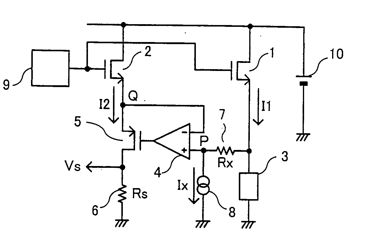
[0047] The drive circuit 9 outputs a common drive signal to the output transistor 1 and the auxiliary transistor 2, thereby turning ON / OFF the output transistor 1 and the auxiliary transistor 2. In the first embodiment, the H level drive signal output from the drive circuit 9 has a high potential capable of sufficiently turning ON the output transistor 1 and the auxiliary transistor 2. Furthermore, the L level drive signal output from the drive circuit 9 has a low potential capable of sufficiently turning OFF the output transistor 1 and the auxiliary transistor 2.

[0048] The operation of the current detection circuit in accordance with the first embodiment shown in FIG. 1 will be described below.

[0049] In the current detection circuit in accordance with the first embodiment shown in FIG. 1, when the potential at the connection point P with respect to the potential at the connection point Q increases in the positive direction by virtue of the differential amplifier 4 and the compensa...

second embodiment

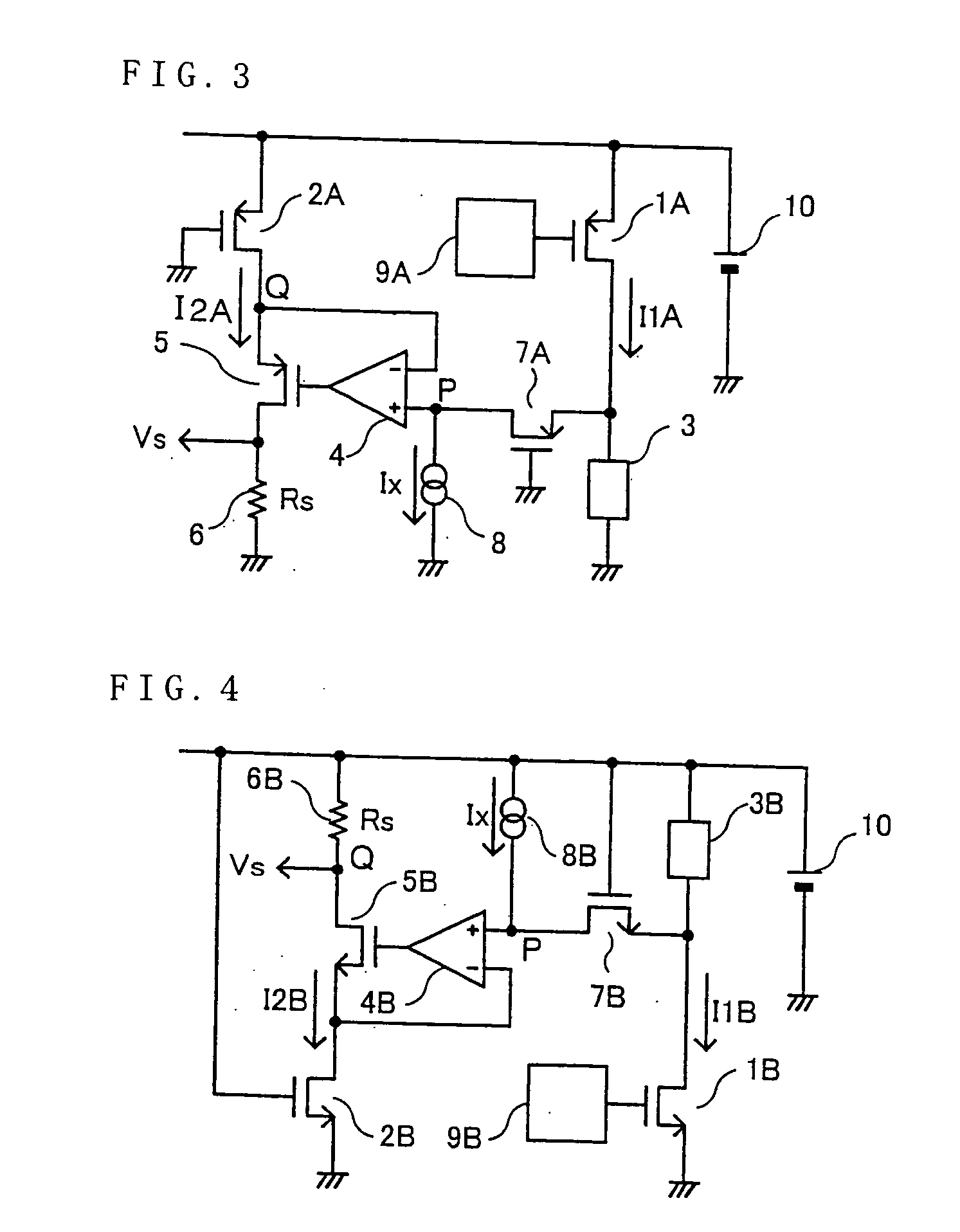
[0061] The current detection circuit in accordance with the second embodiment is produced so as to be built in a monolithic integrated circuit, and the ratio of the size of the output transistor 1A, the size of the auxiliary transistor 2A and the size of the offset resistor device 7A is set at n:1:k. Setting the size ratio at n:1:k is to make the gate lengths of the three transistors equal and to set the ratio of the gate widths of the three transistors at n:1:k, for example.

[0062] The differential amplifier 4 detects the potential difference between the connection point P of the offset resistor device 7A and the current source circuit 8 and the connection point Q of the auxiliary transistor 2A and the compensation transistor 5, and amplifies the potential difference. The differential amplifier 4 then outputs the amplified voltage to the gate of the compensation transistor 5. The drive circuit 9A outputs a drive signal to the gate of the output transistor 1, thereby turning ON / OFF t...

third embodiment

[0070] As shown in FIG. 4, in the current detection circuit in accordance with the third embodiment, a load 3B is connected to the power supply potential side. An output transistor 1B serving as a switching device is formed of an N-channel MIS FET, the source of which is grounded. In FIG. 4, an auxiliary transistor 2B, a compensation transistor 5B and an offset resistor device 7B are all formed of an N-channel MIS FET. The gates of the auxiliary transistor 2B and the offset resistor device 7B have the power supply potential Vi, and the source of the auxiliary transistor 2B is grounded. A current source circuit 8B is configured to pass a current to the offset resistor device 7B, and a current detection resistor 6B is connected to the power supply potential side.

[0071] As described above, the current detection circuit in accordance with the third embodiment has a configuration wherein the connections to the power supply potential side and the ground potential side in the current detec...


PUM


Abstract

A current detection circuit of the present invention has a switching device 1; an auxiliary switching device 2; an offset voltage source comprising an offset resistor device 7 and a current source circuit 8; a compensation circuit, comprising a differential amplifier 4 and a compensation transistor 5, for adjusting the output current of the auxiliary switching device 2 so that the potential obtained by subtracting the voltage drop across the offset resistor device 7 from the output potential of the auxiliary device 1 is equal to the output potential of the auxiliary switching device 2, being configured that the detection level of the current flowing in the switching device 1 is shifted by an offset amount.

Description

BACKGROUD OF THE INVENTION [0001] The present invention relates to a current detection circuit for detecting the current flowing in a switching device, such as a MIS FET (metal insulator semiconductor field effect transistor), and a switching power supply using the same. [0002] In recent years, switching power supplies have been used in various electronic apparatuses because of their high efficiency and high power conversion characteristics. In particular, in the case that quick transient response characteristics are requested, the current mode control system, which is not affected by the resonance frequency of an inductor and an output capacitor constituting such a switching power supply, is used. The current mode control system detects the current flowing in the inductor and controls the current to carry out output control, and requires a current detection circuit. In the case that a current detection device, such as a resistor, is used in a current detection circuit, a conduction...

Claims


Application Information

Patent Timeline
Patent Type & Authority Applications(United States)
IPC IPC(8): G05F3/04
CPCH02M2001/0009H02M3/156H02M1/0009
Inventor RYU, TAKASHIISHII, TAKUYAMOTOMORI, MIKIOTANABE, HIROHISASHIGEMI, TOMOYA
Owner PANASONIC SEMICON SOLUTIONS CO LTD
Why Eureka
Try Eureka