Unified digital architecture

a digital architecture and unified technology, applied in the field of logic architecture, can solve the problems of data transfer bandwidths that typically outpace i/o transfer rates, and the overall system cost associated with the use of parallel data buses tends to be high

Inactive Publication Date: 2006-02-09
IBM CORP
View PDF16 Cites 361 Cited by
  • Summary
  • Abstract
  • Description
  • Claims
  • Application Information

AI Technical Summary

Problems solved by technology

One drawback of such parallel links is the moderate rate of data transmission due to improved microprocessor performance, resulting in data transfer bandwidths that typically outpace I / O transfer rates.
Finally, the overall system cost associated with the use of the parallel data bus tends to be high.

Method used


Image

  • Unified digital architecture
  • Unified digital architecture
  • Unified digital architecture

Examples


Embodiment Construction

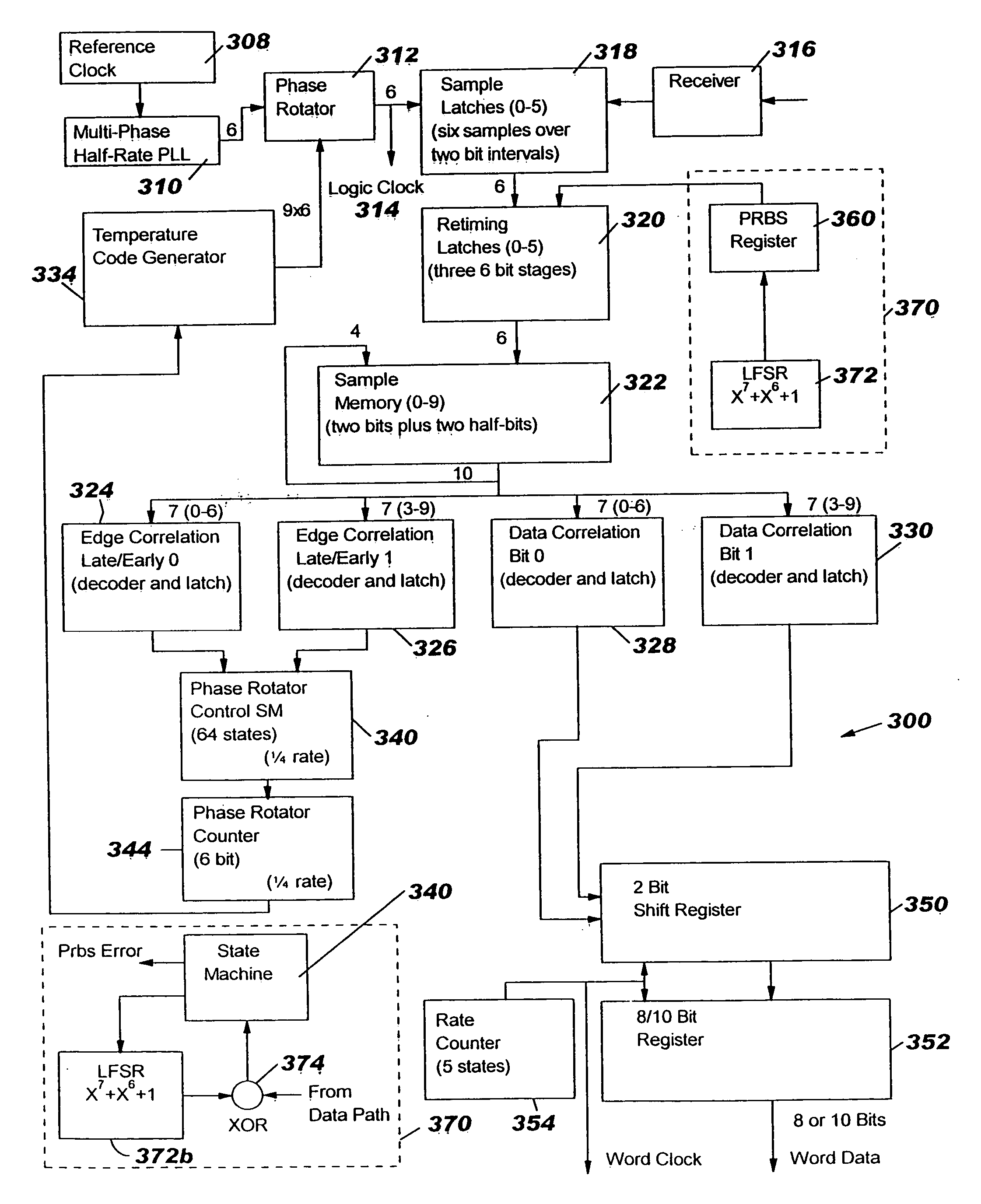
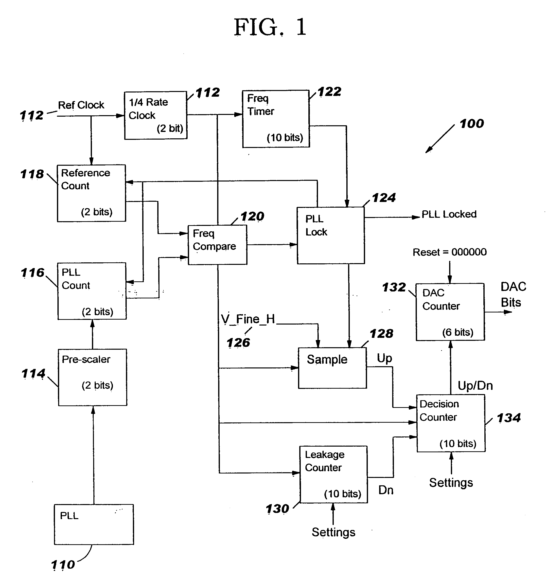
[0013] The PLL control architecture is intended to provide the coarse PLL control loop for a dual-loop PLL. Lock is determined by comparing two Grey counters running on the reference and PLL clocks. The digital to analog conversion (DAC) bits, which set the coarse control voltage for the PLL, are controlled by monitoring a signal from the PLL (V_Fine_H) which indicates which half of its operating range it is in. FIG. 1 illustrates the PLL control circuit.

[0014] More specifically, FIG. 1 shows a full data rate PLL 110. This PLL is the clock source for the transmitted data and runs at the full data rate of e.g. 2 to 3 Gbps. A stable frequency from a reference clock 112 is required for determining if the PLL is locked to its correct frequency. The clock 112 operates at one-fourth of the full data rate. For example, a 625 Mhz clock rate is used for an operational data rate of 2.5 Gbps. A single clock phase is buffered, is brought out of the PLL, and is used to drive into a phase buffer...


PUM


Abstract

A unified, unidirectional serial link is described for providing data across wired media, such as a chip-to chip or a card-to-card interconnect. It consists of a transmit section and a receive section that are operated as pairs to allow the serial data communication. The serial link is implemented as part of a VLSI ASIC module and derives its power, data and clocking requirements from the host modules. The logic transmitter portion contains a phase locked loop (PLL), a dibit data register, a finite impulse response (FIR) filter and a transmit data register. The phase locked loop comprises both a digital coarse loop and an analog fine loop. The digital receiver portion contains a PLL, an FIR phase rotator, a phase rotator control state machine, and a clock buffer. The transmitter and the receiver each preferably utilize a pseudo-random bit stream (PRBS) generator and checker.

Description

RELATED APPLICATIONS [0001] This application is a continuation of application Ser. No. 09 / 996,113, filed Nov. 28, 2001, which claims the benefits of provisional patent application Ser. No. 60 / 262,401, filed Jan. 16, 2001, for “Unilink Digital Architecture”. [0002] This application is related to the following copending applications, all of which are incorporated herein by reference: Ser. No. 09 / 996,091, filed Nov. 28, 2001, for “Architecture For Advanced Serial Link Between Two Cards” (Docket No. RAL920010004US2); Ser. No. 09 / 996,053, filed Nov. 28, 2001, for “Analog Unidirectional Serial Link Architecture” (Docket No. RAL920010005US2); and Ser. No. 09 / 997,587, filed Nov. 28, 2001, for “Apparatus And Method For Oversampling With Evenly Spaced Samples” (Docket No. RAL920010011US2).FIELD OF THE INVENTION [0003] The present invention relates to the logic architecture that provides the digital functions required to enable a unified, unidirectional serial link across wired media, such as ...

Claims


Application Information

Patent Timeline
Patent Type & Authority Applications(United States)
IPC IPC(8): H03D3/24H03L7/08H03L7/095H03L7/099H03L7/10H04L7/033H04L27/00
CPCH03L7/08H03L7/095H04L2027/0067H03L7/10H04L7/0337H03L7/0995H03L7/113G06F13/00
Inventor CRANFORD, HAYDEN CLAVIE JR.NORMAN, VERNON ROBERTSSCHMATZ, MARTIN LEO
Owner IBM CORP
Why Eureka
Try Eureka