
Insulating film, capacitive element and semiconductor storage device including the insulating film, and fabrication methods thereof

Inactive Publication Date: 2006-02-09
PANASONIC CORP
View PDF1 Cites 0 Cited by
  • Summary
  • Abstract
  • Description
  • Claims
  • Application Information

AI Technical Summary

Benefits of technology

[0014] The present invention overcomes the above-described problems of the conventional technique. An objective of the present invention is to provide an insulating film which is formed of a ferroelectric film with no voids and no deterioration in ferroelectric characteristics. Another objective of the present invention is to provide a capacitive element with small current leakage and high breakdown voltage which is formed using the insulating film.
[0047] According to the semiconductor storage device production method of the present invention, the capacitive element is formed using a capacitive element fabrication method of the present invention, and therefore, a semiconductor storage device including a capacitive element with small current leakage and high breakdown voltage can be produced. Thus, miniaturization of the capacitive element can be realized without deteriorating the reliability. As a result, a highly-reliable, densely-integrated semiconductor storage device can readily be realized.

Problems solved by technology

However, in the above-described conventional example, generation of voids in the ferroelectric cannot be prevented although the surface of the ferroelectric film can be smoothed.
As a result, very small voids are generated in the ferroelectric film.
However, when the thickness of the ferroelectric film is decreased for downsizing the capacitive element, the proportion of the voids to the film thickness increases.
This causes a deterioration in the polarization characteristics of the ferroelectric.
Especially when the thickness of the ferroelectric film is 100 nm to 90 nm or less so as to comply with the design rule of 0.18 μm, the influence of the voids is large, resulting in a significant deterioration in ferroelectric characteristics.

Method used


Image

  • Insulating film, capacitive element and semiconductor storage device including the insulating film, and fabrication methods thereof
  • Insulating film, capacitive element and semiconductor storage device including the insulating film, and fabrication methods thereof
  • Insulating film, capacitive element and semiconductor storage device including the insulating film, and fabrication methods thereof

Examples


embodiment 1

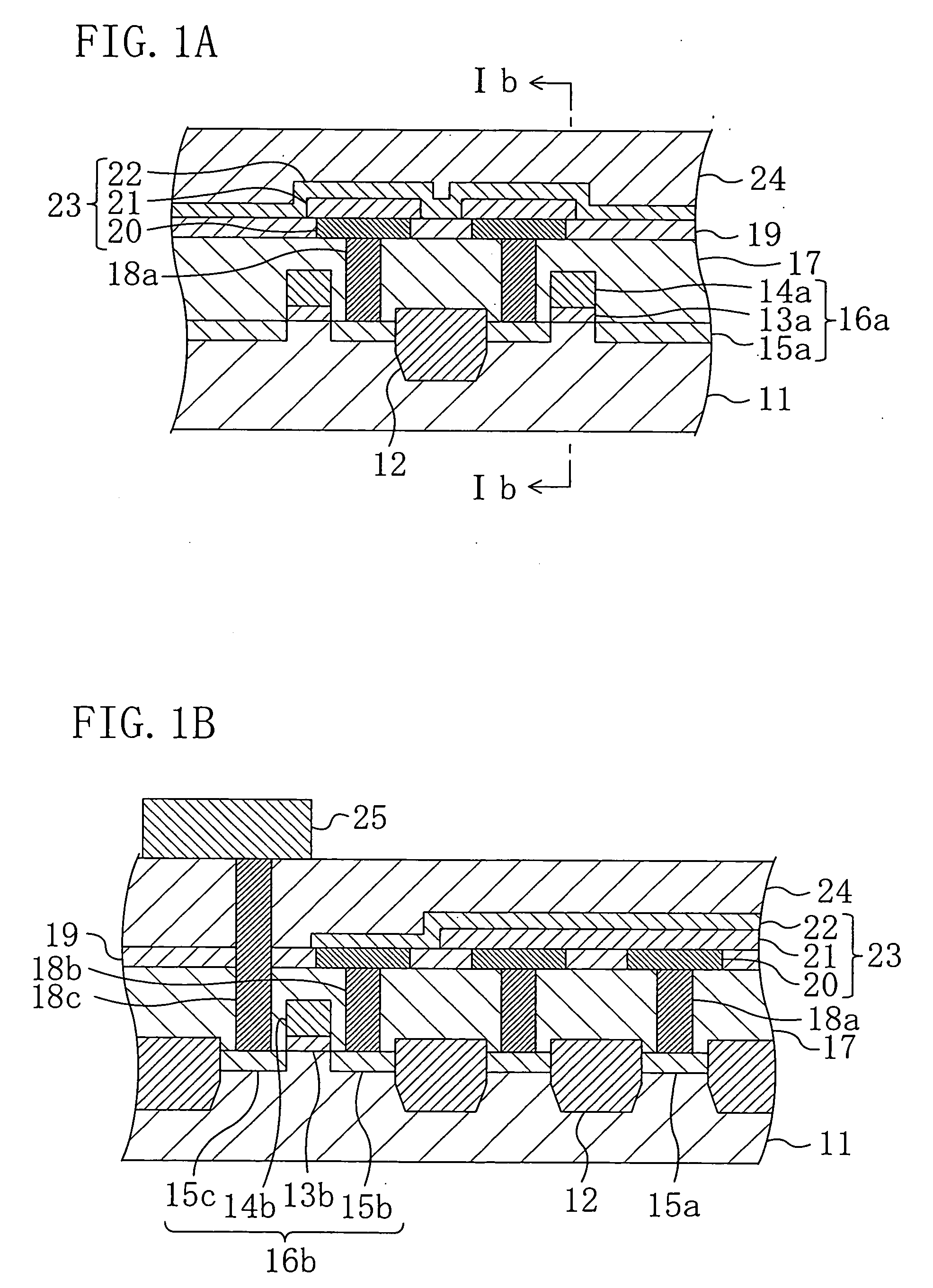
[0065]FIG. 1A and FIG. 1B show principal part of a cross-sectional structure of a semiconductor storage device including a capacitive insulating film according to embodiment 1. FIG. 1A shows a cross section taken along a word line. FIG. 1B shows a cross section taken along line Ib-Ib of FIG. 1A, i.e., taken along a bit line.

[0066] Referring to FIG. 1A and FIG. 1B, memory cell transistors 16a, a memory cell plate driver transistor 16b, and a capacitive element 23 are provided on a semiconductor substrate 11 of silicon.

[0067] Each of the memory cell transistors 16a includes a gate insulating film 13a, a gate electrode 14a and an impurity-diffused region 15a. The semiconductor storage device includes a plurality of memory cell transistors 16a which are arranged in a matrix along the word and bit lines. The memory cell plate driver transistor 16b includes a gate insulating film 13b, a gate electrode 14b and an impurity-diffused region 15b. The memory cell plate driver transistor 16b i...

embodiment 2

[0100] Hereinafter, embodiment 2 of the present invention is described with reference to the drawings.

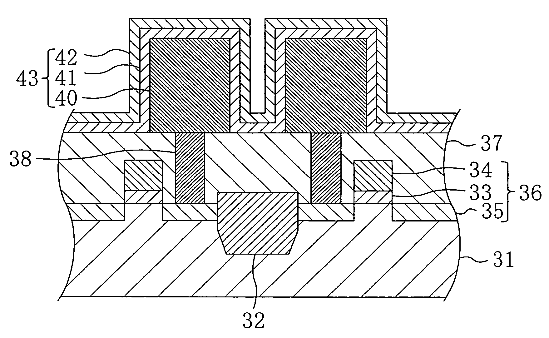
[0101]FIG. 7 shows principal part of a capacitive insulating film of embodiment 2 and a capacitive element and semiconductor storage device including the capacitive insulating film in a cross section taken along a word line. The capacitive element of embodiment 2 has a three-dimensional geometry such that the capacitive insulating film covers not only the upper surface but also the side surface of the lower electrode. More specifically, the capacitive element of embodiment 2 has a so-called “concave” electrode as shown in FIG. 7.

[0102] As shown in FIG. 7, a pair of memory cell transistors 36 and a capacitive element 43 are provided on a semiconductor substrate 32 made of silicon.

[0103] The memory cell transistor 36 includes a gate insulating film 33, a gate insulating film 34 and an impurity-diffused region 35. A device isolation region 32 is provided between the memory cell tran...

embodiment 3

[0124] Hereinafter, embodiment 3 of the present invention is described with reference to the drawings.

[0125]FIG. 10 is a cross-sectional view showing a principal part of capacitive insulating film of embodiment 3 and a capacitive element and semiconductor storage device including the capacitive insulating film in a cross section taken along a word line. The capacitive element of embodiment 2 has a three-dimensional geometry such that the capacitive insulating film covers not only the upper surface but also the side surface of the lower electrode. More specifically, the capacitive element of embodiment 2 has a so-called “convex” electrode as shown in FIG. 10. It should be noted that, in FIG. 10, components equivalent to those of FIG. 7 are denoted by the same reference numerals used in FIG. 7, and the descriptions thereof are herein omitted.

[0126] As shown in FIG. 10, a lower electrode 40 is provided on a first interlayer insulating film 37. The lower electrode 40 has a cylindrical...


PUM


Abstract

A capacitive element comprises: a lower electrode formed above a semiconductor substrate; a capacitive insulating film formed of a ferroelectric on the lower electrode so as to have a thickness of 100 nm or less; and an upper electrode formed on the capacitive insulating element. In any cross section of the capacitive insulating film which is perpendicular to the semiconductor substrate, a sum of the widths of voids generated in the capacitive insulating film which are measured in a direction perpendicular to the thickness direction of the capacitive insulating film is 20% or less of a unit width.

Description

CROSS-REFERENCE TO RELATED APPLICATION [0001] This application claims priority under 35 U.S.C. §119(a) on Japanese Patent Application No. 2004-229021 filed on Aug. 5, 2004, the entire contents of which are hereby incorporated by reference.BACKGROUND OF THE INVENTION [0002] The present invention relates to a ferroelectric insulating film, a capacitive element and semiconductor device including the insulating film, and fabrication methods thereof. [0003] In recent years, a ferroelectric film having spontaneous polarization characteristics has been studied actively for the purpose of realizing practical use of a nonvolatile memory device capable of lower voltage operation and high-speed writing and reading. Especially for the purpose of realizing a semiconductor storage device on the order of megabits on an LSI formed by a CMOS device based on a design rule of 0.18 μm or smaller, a semiconductor device having a stack structure that achieves a large capacity within a small occupation ar...

Claims


Application Information

Patent Timeline
IPC IPC(8): H01L21/00H01L29/94H01L21/8242
CPCH01L27/11502H01L28/65H01L28/55H01L27/11507H10B53/30H10B53/00
Inventor HAYASHI, SHINICHIRONASU, TORU
Owner PANASONIC CORP
Learn More