Gallium nitride based semiconductor light emitting diode and process for preparing the same

a technology of light-emitting diodes and gallium nitride, which is applied in the manufacture of semiconductor/solid-state devices, semiconductor devices, electrical apparatus, etc., can solve the problems of low transparency, lowering the overall light-emission efficiency of the light-emitting diodes of interest, and the inability to easily form ohmic contact with direct vapor deposition of ito on the p-type gan layer, etc., to achieve improved contact resistance and high transparency

Inactive Publication Date: 2006-02-16
SAMSUNG ELECTRO MECHANICS CO LTD
View PDF8 Cites 9 Cited by
  • Summary
  • Abstract
  • Description
  • Claims
  • Application Information

AI Technical Summary

Benefits of technology

[0017] Therefore, the present invention has been made in view of the above problems, and it is an object of the present invention to provide a gallium nitride based semiconductor light emitting diode having high transparency and at the same time, improved contact resistance between the p-type GaN layer and electrode.

Problems solved by technology

However, the transparent electrode layer 15 made of Ni / Au has low transparency of only about 60% to 70% even when it is heat treated, and such low transparency gives rise to lowering the overall light emission efficiency of the light emitting diode of interest when it is used in realizing a package by wire bonding.
However, since ITO is an n-type material, having a work function of 4.7 to 5.2 eV, which is lower than that of p-type GaN, direct vapor-deposition of ITO on the p-type GaN layer does not easily form an ohmic contact.
However, doped Zn or C has high mobility and thus prolonged use of the light emitting diode of interest may cause diffusion of doped Zn or C into the lower part of the p-type GaN layer resulting in problems such as deterioration of reliability of the light emitting diode.
However, such a method may have a disadvantage of exhibiting unstable ohmic contact, depending on forming conditions.

Method used


Image

  • Gallium nitride based semiconductor light emitting diode and process for preparing the same
  • Gallium nitride based semiconductor light emitting diode and process for preparing the same
  • Gallium nitride based semiconductor light emitting diode and process for preparing the same

Examples


Embodiment Construction

[0051] A gallium nitride based semiconductor light emitting diode in accordance with the present invention will now be described in detail with reference to the annexed drawings.

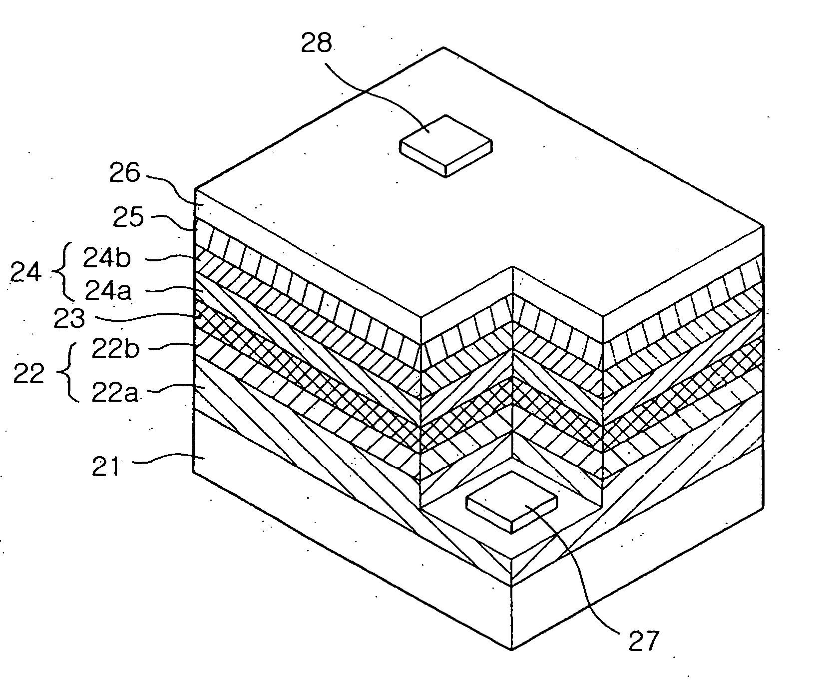
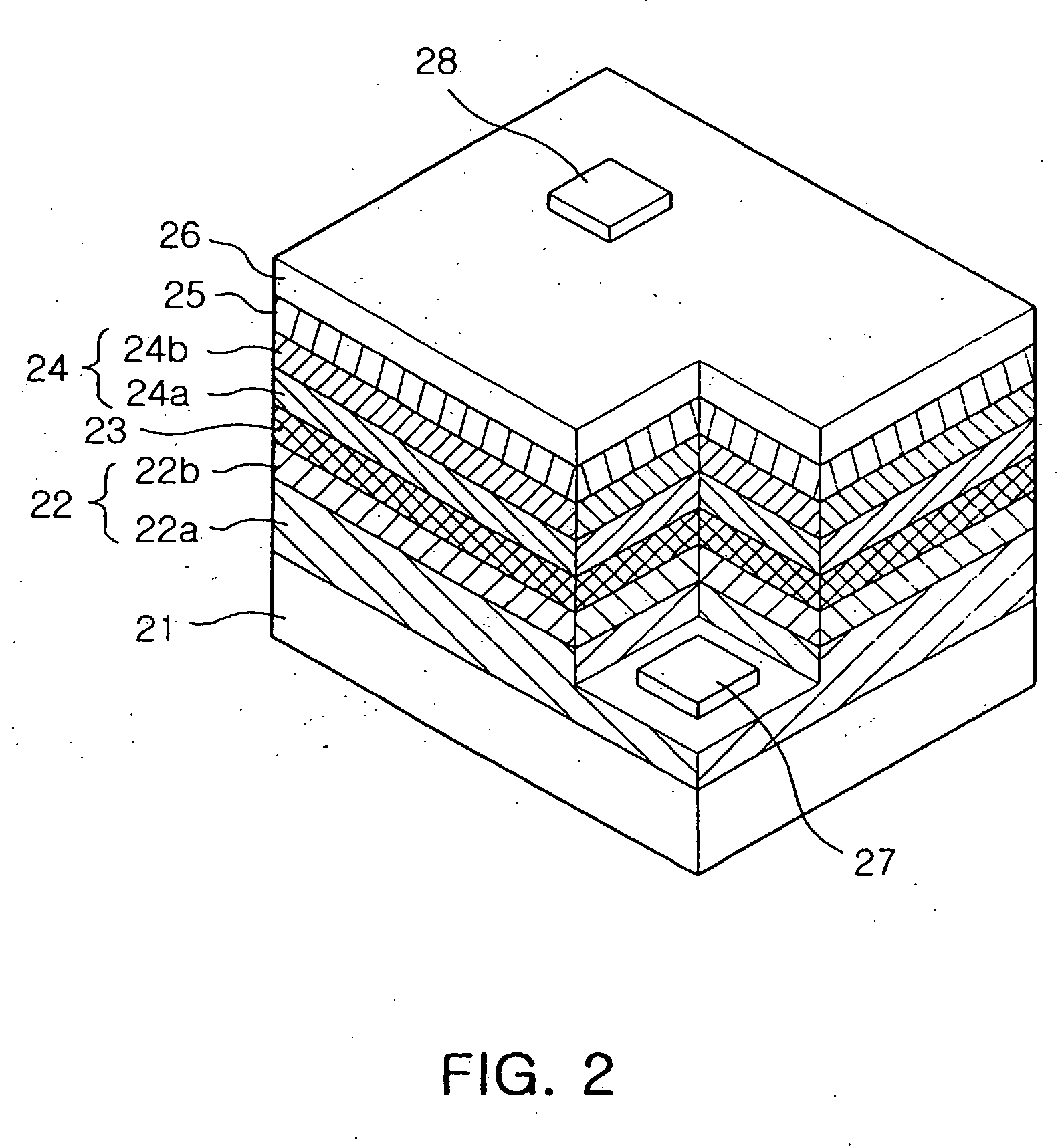
[0052]FIG. 2 is a cross-sectional side view showing a structure of a gallium nitride based semiconductor light-emitting diode in accordance with one embodiment of the present invention.

[0053] As shown in FIG. 2, the gallium nitride based semiconductor light-emitting diode in accordance with the present invention comprises a sapphire substrate 21 for growing the gallium nitride based semiconductor material, and a lower clad layer 22 made of a first conductive semiconductor material, an active layer 23, an upper clad layer 24 made of a second conductive semiconductor material, an ohmic contact forming layer 25, a transparent electrode layer 26 and first and second electrodes 27 and 28, these layers being formed sequentially on the sapphire substrate 21.

[0054] The lower clad layer 22 may be made of an n-type...


PUM

PropertyMeasurementUnit
temperatureaaaaaaaaaa
transparencyaaaaaaaaaa

Abstract

The present invention provides a gallium nitride based semiconductor light emitting diode having high transparency, and at the same time, capable of improving contact resistance between a p-type GaN layer and electrode and a process for preparing the same. These objects can be accomplished by forming, on an upper part of a upper clad layer made of p-GaN, an ohmic contact forming layer using MIO, ZIO and CIO (In2O3 including one of Mg, Zn and Cu), and then a transparent electrode layer and a second electrode with ITO thereon, so as to improve contact resistance between the upper clad layer and the second electrode while providing high transparency.

Description

RELATED APPLICATIONS [0001] The present application is based on, and claims priority from, Korean Application Number 2004-6268.6, filed Aug. 10, 2004, the disclosure of which is hereby incorporated by reference herein in its entirety. BACKGROUND OF THE INVENTION [0002] 1. Field of the Invention [0003] The present invention relates to a gallium nitride based semi-conductor light emitting diode, and more particularly to a gallium nitride based semiconductor light emitting diode having good luminance characteristics while being capable of operating at a low drive voltage by improving transparency of an electrode and at the same time, forming a good quality ohmic contact between a transparent electrode layer and upper clad layer, and a process for preparing the same. [0004] 2. Description of the Related Art [0005] Recently, a great deal of attention has been directed to light emitting diodes using a gallium nitride (GaN) based semiconductor as a backlight source of a flat display device...

Claims


Application Information

Patent Timeline
Patent Type & Authority Applications(United States)
IPC IPC(8): H01L29/221H01L33/10H01L33/06H01L33/32H01L33/38H01L33/42
CPCH01L21/28575H01L29/452H01L33/42H01L33/40H01L33/32H01L2924/10155
Inventor CHAE, SEUNG WANKWAK, JUN SUBSHIN, HYOUN SOOSEO, JUN HO
Owner SAMSUNG ELECTRO MECHANICS CO LTD
Why Eureka
Try Eureka