Cross point array cell with series connected semiconductor diode and phase change storage media

a semiconductor diode and phase change technology, applied in the direction of digital storage, material nanotechnology, instruments, etc., can solve the problems of unselected leakage and increase the cost of the device, and achieve the effect of reducing leakage phase change materials

Inactive Publication Date: 2006-02-16
IBM CORP
View PDF10 Cites 142 Cited by
  • Summary
  • Abstract
  • Description
  • Claims
  • Application Information

AI Technical Summary

Benefits of technology

[0009] It is a purpose of the invention to reduce leakage phase change material in memory cells;
[0010] It is another purpose of the invention to eliminate half select cell leakage phase change material in memory cells.

Problems solved by technology

For a typical integrated circuit (IC) chip, this unselected leakage is exacerbated by the size of the particular array and, correspondingly, the number of leaking cells.

Method used


Image

  • Cross point array cell with series connected semiconductor diode and phase change storage media
  • Cross point array cell with series connected semiconductor diode and phase change storage media
  • Cross point array cell with series connected semiconductor diode and phase change storage media

Examples


Embodiment Construction

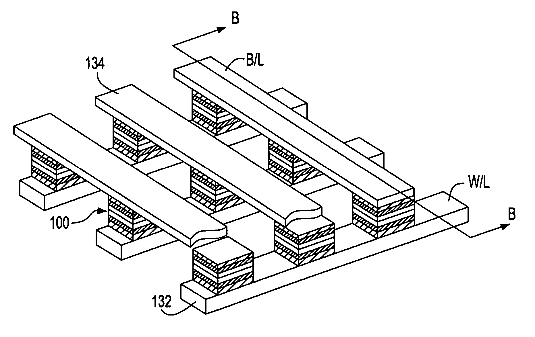
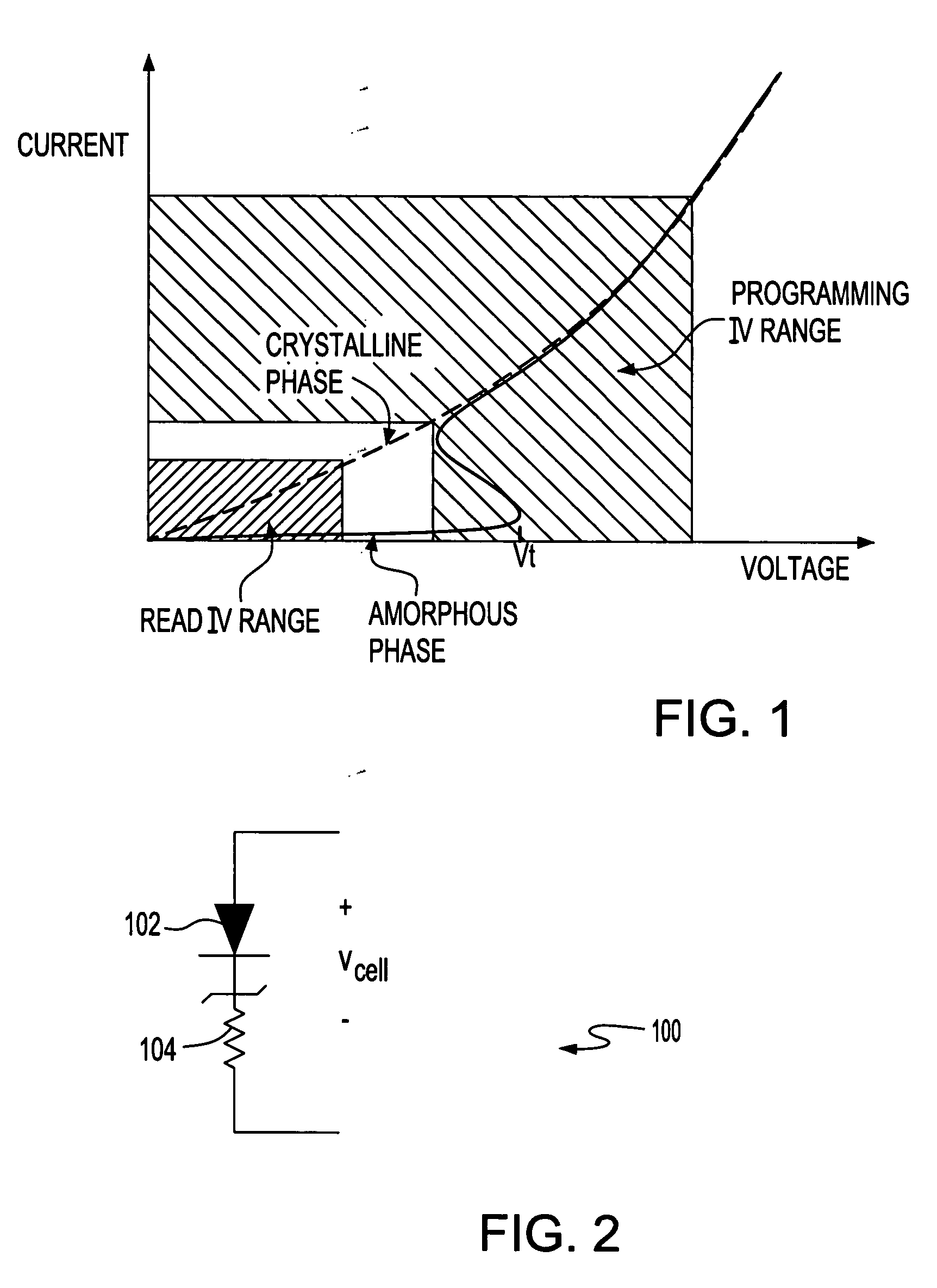
[0020] Turning now to the drawings and more particularly FIG. 2 shows an example of a preferred embodiment low leakage nonvolatile storage device 100 according to the present invention, e.g., a nonvolatile cell in a cross point storage array of low leakage cells. In particular, each preferred embodiment low leakage storage cell 100 includes a semiconductor diode 102, preferably a vertical diode in a semiconductor nanowire, in series with storage media 104, e.g., chalcogenide phase change material. Each low leakage cell 100 has at least two states; preferably, a resistive state wherein the vertical diode 102 is in series with resistive crystalline phase change storage media 104; and, a stepped state with the stepped resistance of the amorphous phase change storage media 104 in series with the vertical diode 102. For examples of phase material cells in a cross point array and switching phases to switch between electrical states, see e.g., U.S. application Ser. No. 10 / 732,582 entitled ...


PUM


Abstract

A storage cell that may be a memory cell, and an integrated circuit (IC) chip including an array of the memory cells and a method of forming the IC. Each storage cell includes a series connected diode and storage media formed between a top an bottom electrode. The diode is a vertical diode and may be formed in a semiconductor nanowire.

Description

CROSS REFERENCE TO RELATED APPLICATION [0001] The present invention is related to U.S. application Ser. No. 10 / 732,582 entitled “FIELD EMISSION PHASE CHANGE DIODE MEMORY” to Stephen S. Furkay et al. and to U.S. application Ser. No. 10 / 732,580 entitled “PHASE CHANGE TIP STORAGE CELL” to David V. Horak et al., both filed Dec. 10, 2003 and assigned to the assignee of the present invention.BACKGROUND OF THE INVENTION [0002] 1. Field of the Invention [0003] The present invention is related to nonvolatile solid state storage and particularly to an integrated circuit (IC) chip with an array of non volatile solid state storage cells with a phase change material memory element. [0004] 2. Background Description [0005] Solid state phase change materials that are chalcogen (Group VI elements such as sulfur (S), selenium (Se) and tellurium (Te)) alloys with at least one of germanium (Ge), arsenic (As), silicon (Si), and antimony (Sb)) are known as chalcogenides and are well known. Chalcogenides ...

Claims


Application Information

Patent Timeline
Patent Type & Authority Applications(United States)
IPC IPC(8): G11C11/00
CPCB82Y10/00B82Y30/00G11C13/0004G11C13/0007G11C13/0014G11C13/0016H01L27/2463G11C2213/31G11C2213/72H01L45/06H01L45/1233H01L45/141H01L27/2409G11C2213/16H10B63/20H10B63/80H10N70/882H10N70/231H10N70/826
Inventor LAM, CHUNG H.WONG, HON-SUM P.
Owner IBM CORP
Why Eureka
Try Eureka