Method and apparatus for jitter analysis and program therefor

a jitter analysis and program technology, applied in the field of methods, apparatuses and programs for analyzing jitter, can solve problems such as lack of a method, an apparatus or a program

Inactive Publication Date: 2006-02-16
NEC ELECTRONICS CORP
View PDF7 Cites 25 Cited by
  • Summary
  • Abstract
  • Description
  • Claims
  • Application Information

AI Technical Summary

Problems solved by technology

However, there lacks up to now a method, an apparatus or a program whereby both the power supply noise generated and the jitter attributable thereto may be comprehensively analyzed within a reasonable length of time.

Method used


Image

  • Method and apparatus for jitter analysis and program therefor
  • Method and apparatus for jitter analysis and program therefor
  • Method and apparatus for jitter analysis and program therefor

Examples


first embodiment

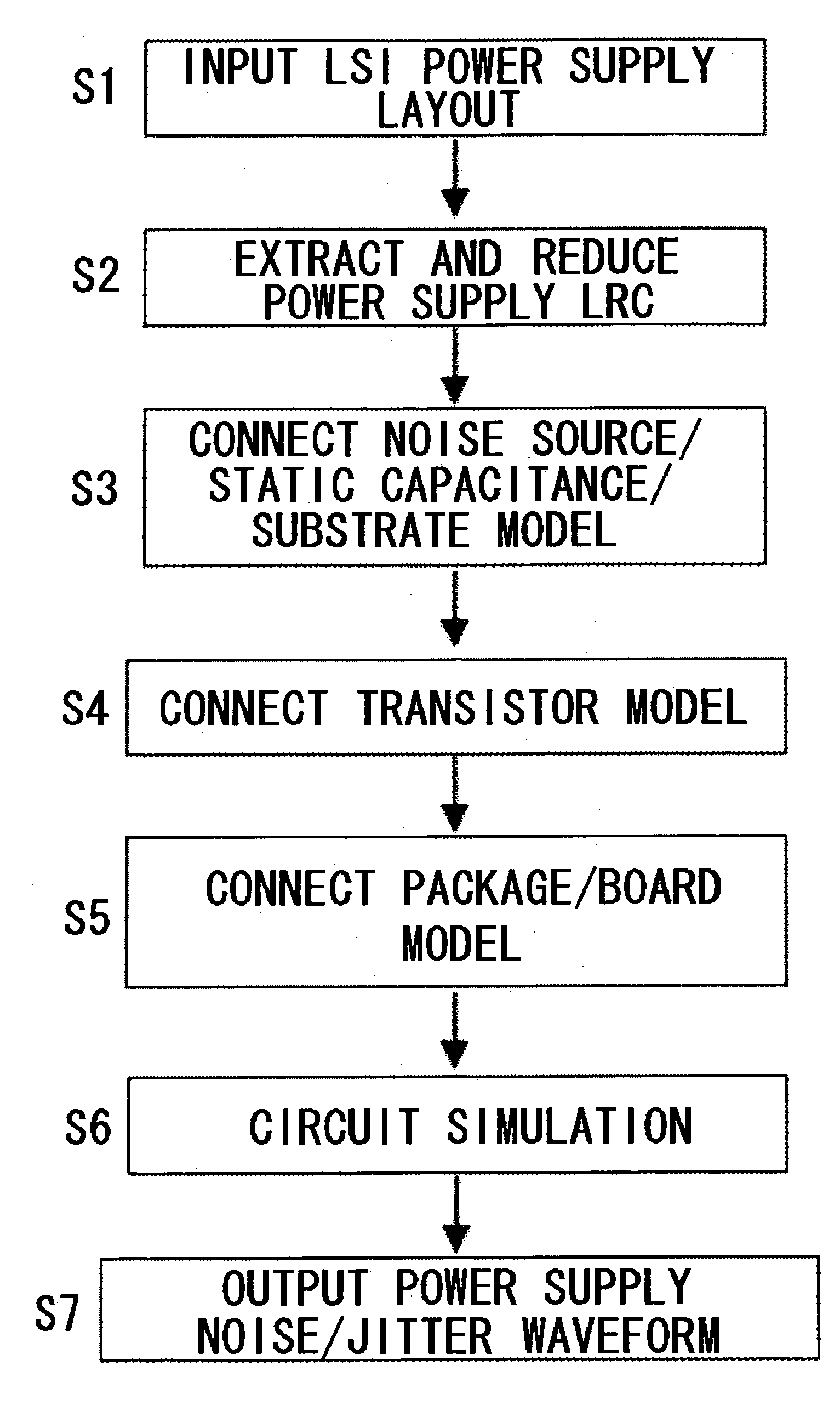
[0039]FIG. 6 depicts a block diagram of an apparatus for jitter analysis according to a first embodiment of the present invention. Power supply layout extraction means 602, power supply LRC extraction means 604 and reducing means 605 together make up power supply analysis model extraction means adapted for extracting interconnection resistance, interconnection capacitance and interconnection inductance to output a power supply LRC model. The power supply layout extraction means 602 extracts the layout of the power supply interconnection from LSI layout design data 601 to output a power supply layout data 603. The power supply LRC extraction means 604 extracts the interconnection resistance, interconnection capacitance and the interconnection inductance of the power supply from power supply layout data 603 to form a power supply LRC model. The reducing means reduces the power supply LRC model as necessary to output a reduced power supply LRC model 606.

[0040] An analysis model formul...

second embodiment

[0056] A second embodiment of the present invention will now be explained. FIG. 8 depicts a block diagram of an apparatus for jitter analysis according to the second embodiment of the present invention.

[0057] In the second embodiment, the blocks similar in configuration and operation to those of the jitter analysis apparatus of the first embodiment are denoted by the same reference numerals as those of the first embodiment, and the corresponding description is omitted for simplicity. The jitter analysis apparatus of the second embodiment differs from the apparatus of the first embodiment in that analysis model formulating means 812 separately outputs a model for analysis of the power supply model 813 and a model for jitter analysis 817, and in that analysis executing means 814 causes power supply noise waveform data 816, obtained as a result of the circuit simulation, to be stored in e.g. a file, and exploits the power supply noise waveform data 816, stored in e.g. the file, as inp...

third embodiment

[0071] A third embodiment of the present invention will now be explained. FIG. 21 shows a functional-block-based jitter analysis model of the third embodiment of the present invention, FIG. 22 depicts a flowchart for illustrating the jitter analysis method, and FIG. 23 is a block diagram showing an apparatus for carrying out jitter analysis.

[0072] Referring first to FIG. 23, the configuration of the jitter analysis apparatus according to the third embodiment will now be explained. The present third embodiment differs from the first and second embodiments in that, for the functional blocks, as the subject of jitter analysis, data of correlation among the input signal waveform, power supply noise waveform and jitter characteristics are registered at the outset as jitter correlation data 920. It is noted that, although analysis means 914 carries out simulation for finding the power supply noise waveform, it does not have to carryout circuit simulation for jitter analysis, and hence it...


PUM


Abstract

A method, an apparatus and a program for comprehensively analyzing the power supply noise and consequent jitter for external output signals of the LSI in real time. From LSI layout designing data 601, the resistance, capacitance and inductance of the power supply interconnection are extracted to formulate a power supply LRC model 606. An analysis model formulating unit 812 connects a transistor model 610, a noise source model 607, a silicon substrate model 608 and a package / board (printed circuit board) model 611 to formulate a model for analysis of the power supply noise 813 and a model for jitter analysis 817. An analysis unit 814 acquires power supply noise waveform data 816 by first simulation and also acquires jitter analysis data 815 using power supply noise waveform data 816 by second simulation.

Description

FIELD OF THE INVENTION [0001] This invention relates to a method, an apparatus and a program for analyzing the jitter. More particularly, it relates to a method, an apparatus and a program for analyzing the jitter ascribable to the noise of the power supply of a semiconductor integrated circuit. BACKGROUND OF THE INVENTION [0002] In keeping up with increase in the system operating speed in recent years, the necessity for jitter analysis is increasing. In particular, in keeping up with increase in the data communication speed among LSIs (large scale integrated circuits), the need for analyzing the jitter (I / O jitter) of LSI output signals is increasing. In such analysis, it is necessary to analyze the power supply noise as a major factor responsible for jitter. FIG. 2 depicts a circuit diagram indicating that jitter may be produced by the power supply noise. In the circuit of FIG. 2, clock signals generated in a PLL unit 21, are distributed, by a clock tree 22, and the clock signals ...

Claims


Application Information

Patent Timeline
Patent Type & Authority Applications(United States)
IPC IPC(8): G06F17/50
CPCG06F2217/78G06F17/5036G06F30/367G06F2119/06
Inventor KOBAYASHI, SUSUMU
Owner NEC ELECTRONICS CORP
Why Eureka
Try Eureka