Strained semiconductor-on-insulator structures and methods for making strained semiconductor-on-insulator structures
- Summary
- Abstract
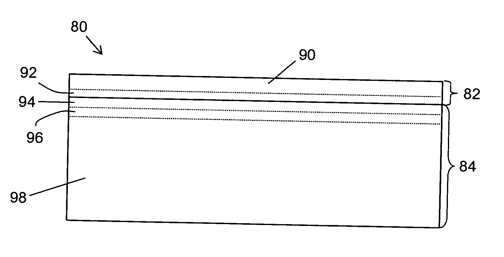
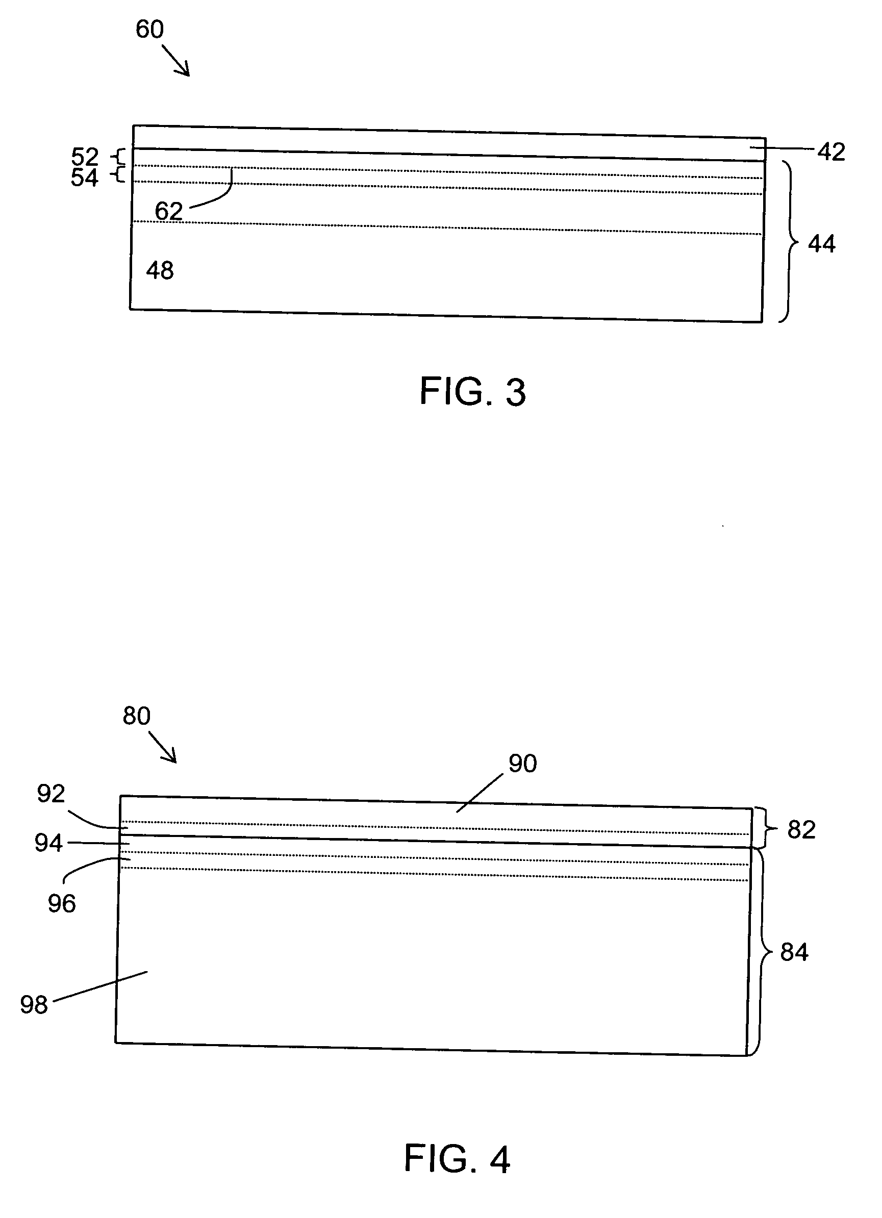
- Description
- Claims
- Application Information
AI Technical Summary
Benefits of technology
Problems solved by technology
Method used
Image

Examples
example
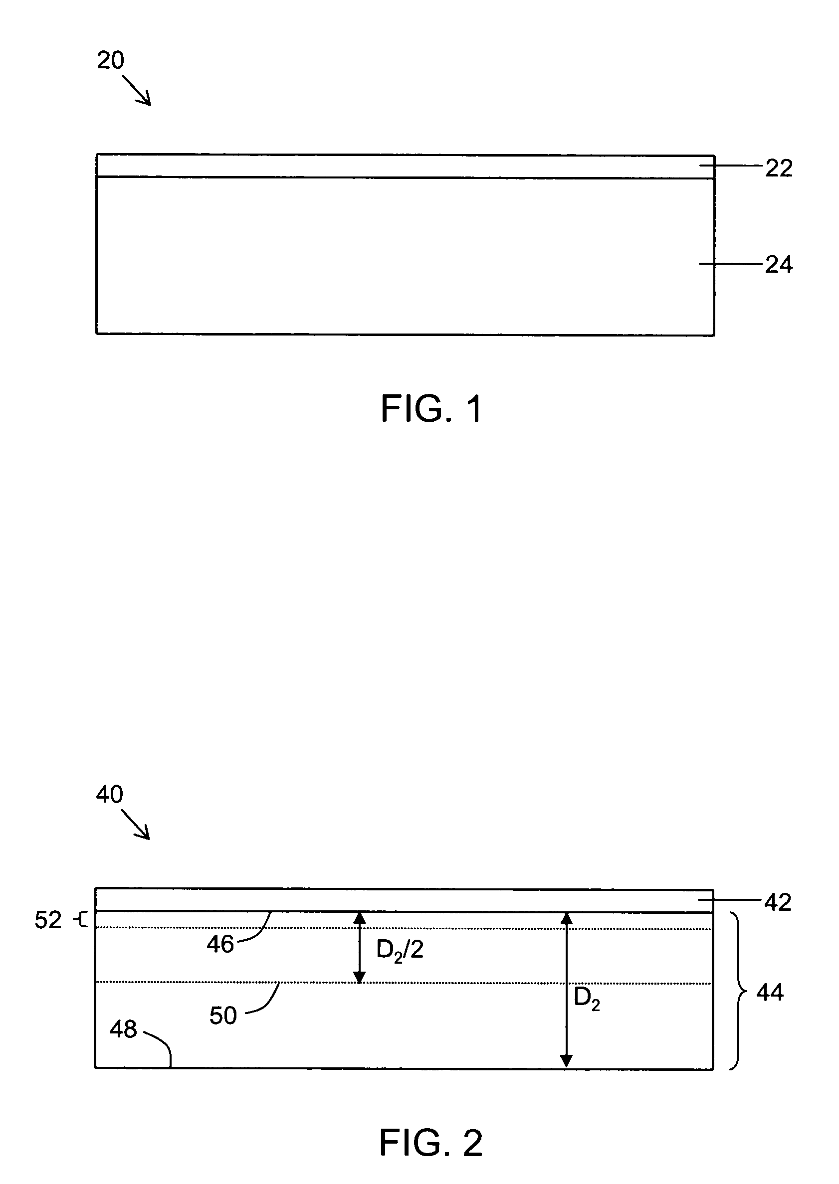
[0125] A 100 mm diameter, 1 mm thick wafer of glass 3N of Table 3 was polished to smoothness. A silicon wafer 525 μm in thickness was implanted with hydrogen at 100 keV and an ion dosage of 8×10¹⁶ ions / cm2 was cleaned with detergent and distilled water followed by a 10% nitric acid wash, and brought into contact with the glass wafer in a SUSS MICROTEC bonder. The glass wafer was heated at 450° C. and the silicon wafer at 400° C. in vacuum, and 10 psi pressure and 1750 V potential difference (glass at ground, silicon wafer at 1750 V) was applied for five minutes. While under the same potential difference and pressure, the glass wafer was heated at 575° C. and the silicon wafer at 525° C. for ten minutes, after which time the potential difference and pressure were removed, and the bonded wafers allowed to cool down. The cooled wafers separated into a silicon-on-glass wafer with a thin silicon layer, and a silicon wafer. The silicon layer on the glass had a thin, damaged top layer, and...
PUM
 Abstract
Description
Claims
Application Information
 - Generate Ideas
- Intellectual Property
- Life Sciences
- Materials
- Tech Scout
- Unparalleled Data Quality
- Higher Quality Content
- 60% Fewer Hallucinations
Browse by: Latest US Patents, China's latest patents, Technical Efficacy Thesaurus, Application Domain, Technology Topic, Popular Technical Reports.
© 2025 PatSnap. All rights reserved.Legal|Privacy policy|Modern Slavery Act Transparency Statement|Sitemap|About US| Contact US: help@patsnap.com