Differential voltage measuring apparatus and semiconductor testing apparatus

Inactive Publication Date: 2006-02-23
ADVANTEST CORP
View PDF3 Cites 15 Cited by
  • Summary
  • Abstract
  • Description
  • Claims
  • Application Information

AI Technical Summary

Benefits of technology

[0136] means for performing measurement by applying gradual voltages to both ends of each of at least the first resistance and the second resistance included in the offset voltage giving means (e.g., offset voltage giving circuits 300, 300b, 300c, 300d, 300e and 300f) before a test of a DUT;
[0137] means for specifying a deviation of non-linear characteristic data of the obtained resistance from an ideal resistance; and
[0138] means for performing linear correction with respect to

Problems solved by technology

When mounting these circuits on a silicon substrate, there is a problem that a manufacturing process of the silicon substrate becomes complicated, laser trimming is required or a chip size is increased in order to realize highly accurate measurement.
There is a problem that this error value results in a serious measurement error factor.
Therefore, since the resistances R1 to R4 for voltage division complicatedly vary due to the common mode voltage Va as well as the potential difference Vx of Va−Vb in the above-described circuit, there is a problem that resistances with good characteristics which are formed of nickel chrome or the like are required.
However, there is adversely a problem that an AD converter having a high-input voltage range and a high resolution is required for-the AD converter 45.
For example, in cases where measurement is carried out with a resolution of ±0.1% (±1000) when the potential difference Vx is 1 Vmax, a 11-bit resolution (±1000) can suffice if a test voltage VS is 1 V. However, there is a problem t

Method used


Image

  • Differential voltage measuring apparatus and semiconductor testing apparatus
  • Differential voltage measuring apparatus and semiconductor testing apparatus
  • Differential voltage measuring apparatus and semiconductor testing apparatus

Examples


Example

[0151] An embodiment to which the present invention is applied will now be described hereinafter with reference to the accompanying drawings. Further, claims are not restricted by an explanation content of the following embodiment, and elements, connection relationships and others described in the embodiment are not necessarily required for the solution means. Furthermore, descriptions / conformations of elements, connection relationships and others written in the embodiments are an example, and the present invention is not restricted to contents of the descriptions / conformations.

[0152] The present invention will now be described hereinafter with reference to FIGS. 3 to 9. It is to be noted that like reference numerals denote elements corresponding to conventional structures, and the explanation of tautological parts will be eliminated.

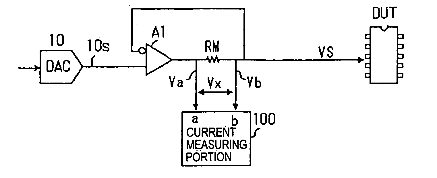
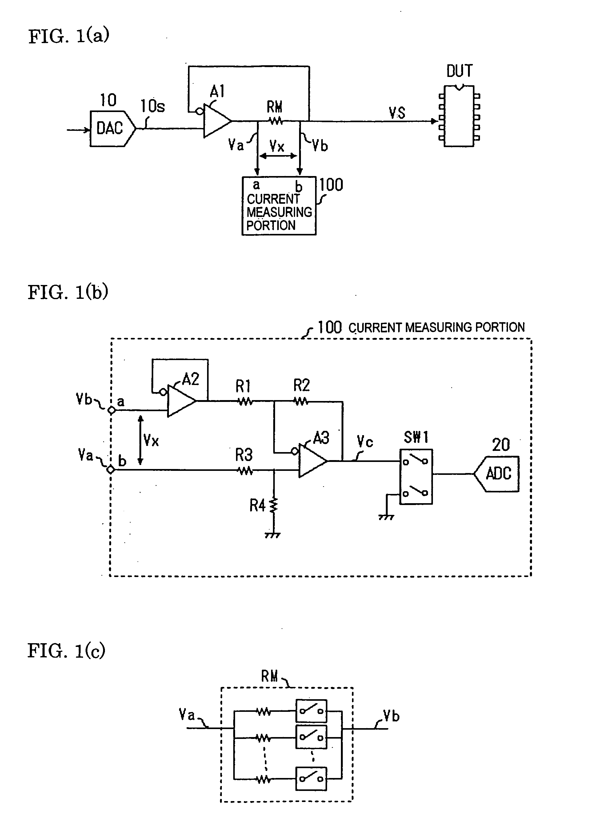
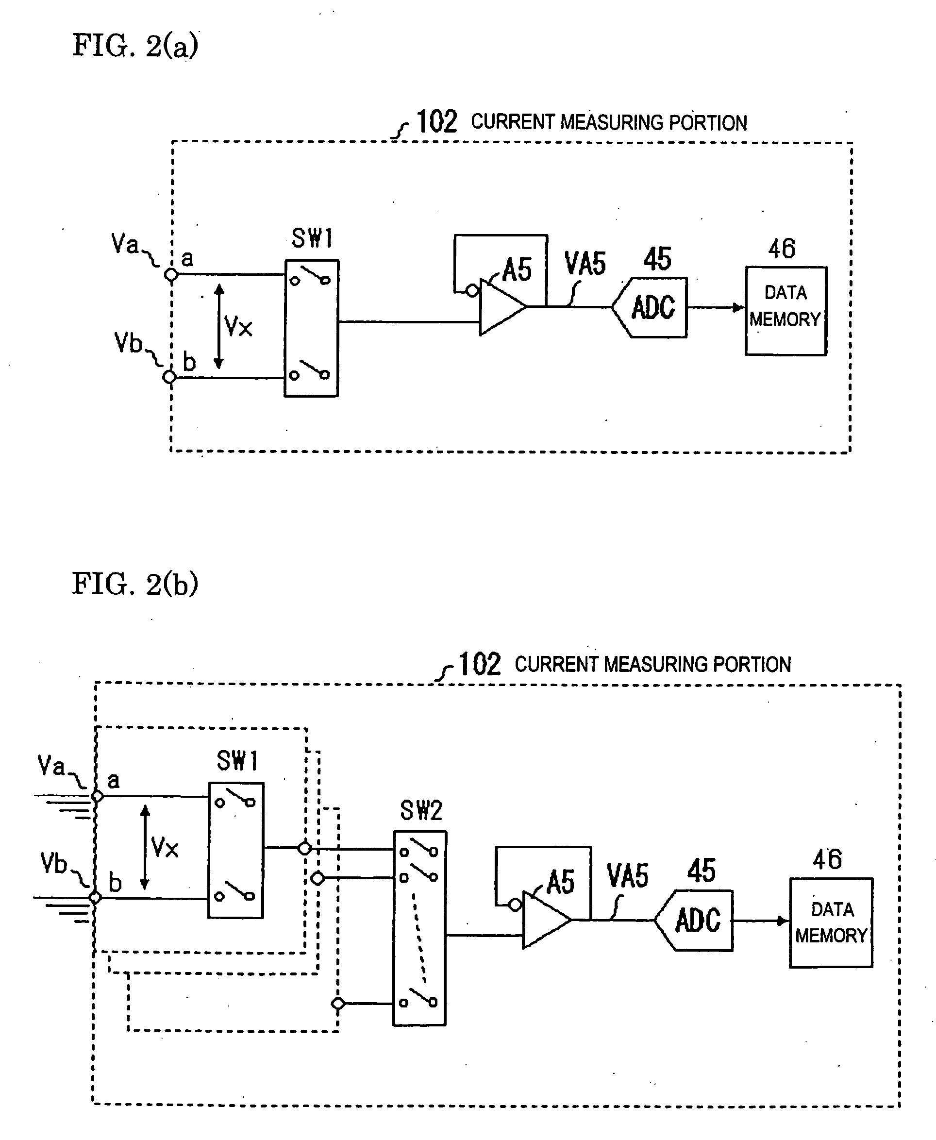
[0153]FIG. 3 shows a primary structural example of a current measuring portion which measures a current of an IC pin of a DUT having a plurality of c...


PUM


Abstract

There is provided a semiconductor testing apparatus comprising a current measuring portion which converts a load current quantity at the time of application of a relatively high test voltage to a DUT to fall within a low-voltage range, and then subjects the low-voltage range to quantization conversion with a predetermined measurement resolution even when the relatively high test voltage is applied to the DUT. This is a differential voltage measuring apparatus comprising: an applied voltage source which applies a predetermined constant voltage to a load device; current/voltage converting means for directly inserting a predetermined resistance between an output end of the applied voltage source and the load device, and converts a quantity of a current flowing through the load device into a voltage; and current measuring means which switches and receives a common mode voltage and a detection voltage in time series, shifts the received voltages to predetermined low voltages, and outputs low-voltage measurement data obtained by receiving each of the shifted voltages and subjecting this voltage to quantization conversion.

Description

TECHNICAL FIELD [0001] The present invention relates to a semiconductor testing apparatus comprising a current measuring portion which can apply a relatively high test voltage to a device under test (DUT) and subject a load current quantity in this application to quantization conversion with a predetermined measurement resolution. More particularly, the present invention relates to a semiconductor testing apparatus comprising a voltage source and current measurement (VSIM) which has a current measuring portion which can perform quantization conversion with a predetermined measurement resolution without being dependent on a high test voltage which is applied to a DUT. BACKGROUND ART [0002] In case of highly accurately measuring a direct-current voltage or a direct current of a device under test (DUT) by a semiconductor testing apparatus, each accurate component is required in an operational amplifier, a peripheral resistance, an AD converter and others. [0003] When mounting these cir...

Claims


Application Information

Patent Timeline
IPC IPC(8): G01R31/26G01R19/00G01R19/10G01R31/28G01R31/30
CPCG01R31/3004G01R19/10
Inventor HASHIMOTO, YOSHIHIRO
Owner ADVANTEST CORP
Why Eureka
Try Eureka