Memory address repair without enable fuses

a memory address and fuses technology, applied in the field of memory systems, can solve the problems of power being required to read fuses, single defective memory locations are not repaired, and there is a near 100% chance that any one memory device or chip will have multiple defective bits, so as to reduce the number of fuses, save space on the memory chip real estate, and save power consumption

Active Publication Date: 2006-02-23
MICRON TECH INC
View PDF5 Cites 14 Cited by
  • Summary
  • Abstract
  • Description
  • Claims
  • Application Information

AI Technical Summary

Benefits of technology

[0028] The present disclosure teaches a memory chip design methodology wherein fuse banks on the memory chip may be implemented without enable fuses. A fuse bank may be enabled by using one or more least significant bits (LSBs) in the memory address stored in the fuse bank, thereby avoiding the need for a separate enable fuse. A reduction in the number of fuses results in space savings on the memory chip real estate and also savings in power consumption because of fewer fuses to be blown and read. With reduced fuse count, the yield of the memory chip's die may also be improved because of less number of defective fuses or failed fuse blows. The use of effective default state inversion for address fuses may further reduce the average number of fuses that need to be blown to repair a given non-redundant memory address.

Problems solved by technology

With such large numbers of bits, there is nearly a 100% chance that any one memory device or chip will have multiple defective bits.
Therefore, typically, single defective memory locations are not repaired by selecting the row and column of that bad location, but rather by replacing an entire row or column of memory elements with a redundant row or column.
Some issues associated with the fuses on a memory chip are: (1) Power is required to read the fuses.
However, if a voltage is applied to a short circuited fuse, then current flows and power is consumed.
(2) It takes time to blow or “program” the fuses.
Programming a fuse is a relatively fast operation, but when each semiconductor die requires a unique pattern of thousands of fuse blows, the time adds up.
(4) With tens of thousands of fuses on the die, there is a growing potential for defective fuses or failed fuse blows, which limit die yield.
However, there would still be some banks with enable fuses to specifically allow the repair of address zero because no address fuses are blown for this address of all zeros and, hence, no enable condition may be detected without the enable fuse.
Likewise, in the case where the default address condition for fuses is to match a high address, there would be no way to selectively repair an address of all 1's.

Method used


Image

  • Memory address repair without enable fuses
  • Memory address repair without enable fuses
  • Memory address repair without enable fuses

Examples


Embodiment Construction

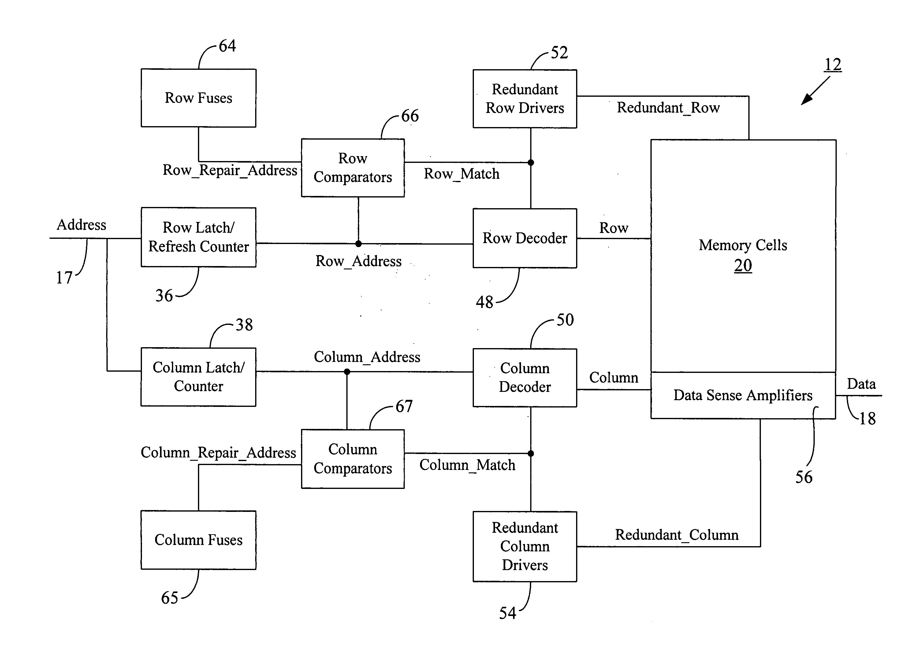
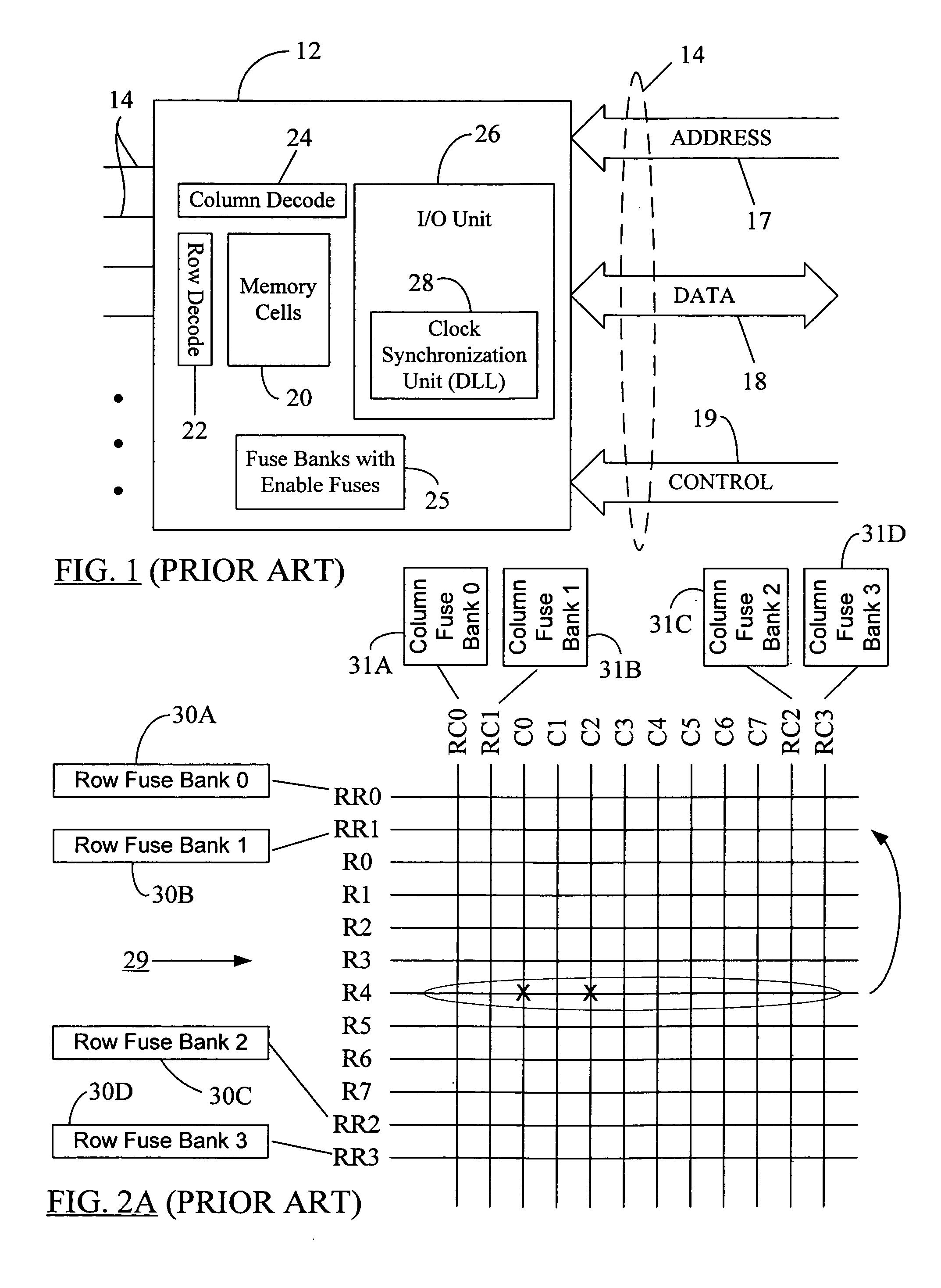
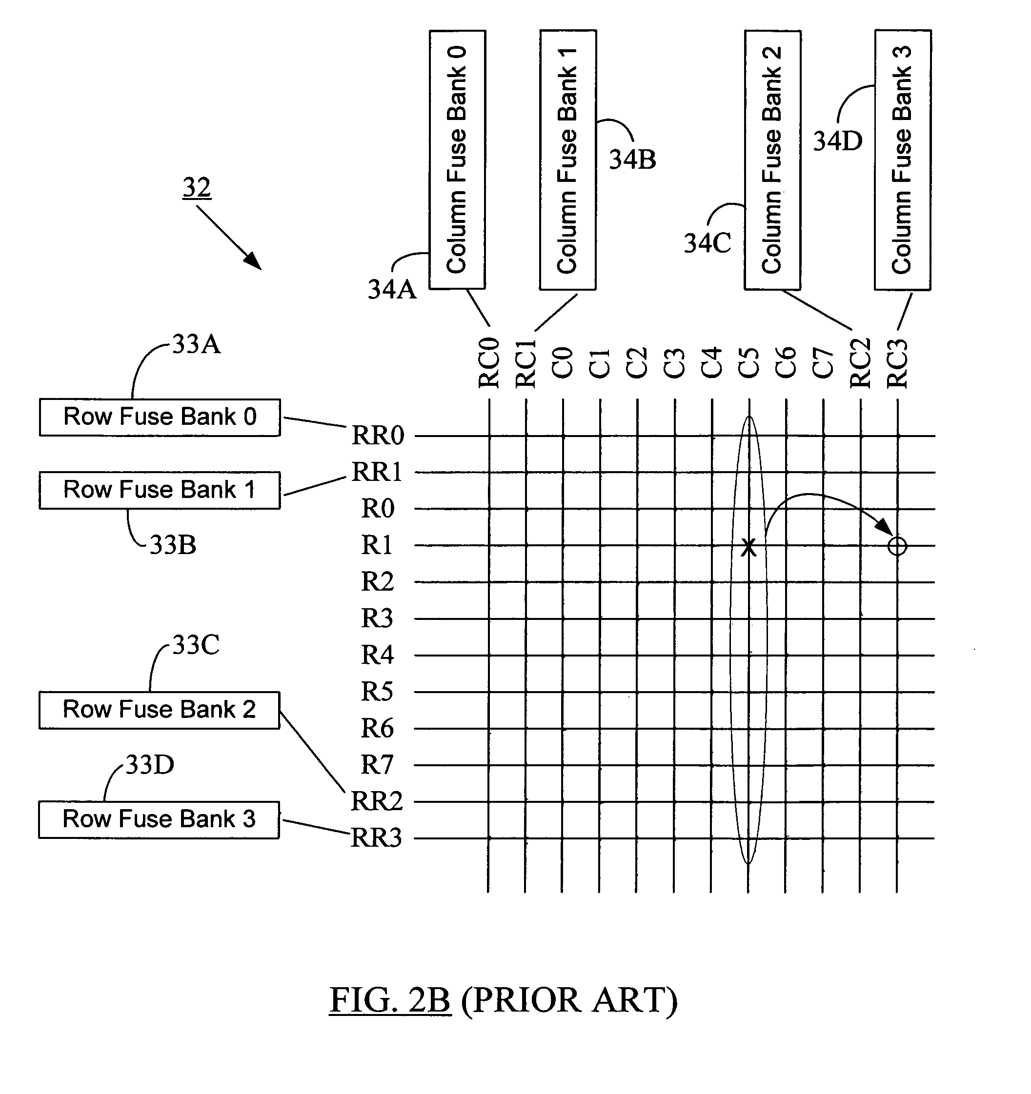
[0042] Reference will now be made in detail to certain embodiments of the present disclosure, examples of which are illustrated in the accompanying figures. It is to be understood that the figures and descriptions of the present disclosure included herein illustrate and describe elements that are of particular relevance to the present disclosure, while eliminating, for the sake of clarity, other elements found in typical data storage or memory systems. It is noted at the outset that the terms “connected”, “connecting,”“electrically connected,” etc., are used interchangeably herein to generally refer to the condition of being electrically connected. It is further noted that various block diagrams and circuit diagrams shown and discussed herein employ logic circuits that implement positive logic, i.e., a high value on a signal is treated as a logic “1” whereas a low value is treated as a logic “0.” However, any of the circuit discussed herein may be easily implemented in negative logi...


PUM


Abstract

A memory chip design methodology is disclosed wherein fuse banks on the memory chip may be implemented without enable fuses. A fuse bank may be enabled by using one or more least significant bits (LSBs) in the memory address stored in the fuse bank, thereby avoiding the need for a separate enable fuse. A reduction in the number of fuses results in space savings on the memory chip real estate and also savings in power consumption because of fewer fuses to be blown and read. With reduced fuse count, the yield of the memory chip's die may also be improved because of less number of defective fuses or failed fuse blows. The use of effective default state inversion for address fuses may further reduce the average number of fuses that need to be blown to repair a given non-redundant memory address. Because of the rules governing abstracts, this abstract should not be used to construe the claims.

Description

BACKGROUND [0001] 1. Field of the Disclosure [0002] The present disclosure generally relates to memory systems and, more particularly, to a system and method to repair memory addresses without enable fuses. [0003] 2. Brief Description of Related Art [0004]FIG. 1 is a simplified block diagram showing a memory chip or memory device 12. The memory chip 12 may be part of a DIMM (dual in-line memory module) or a PCB (printed circuit board) containing many such memory chips (not shown in FIG. 1). The memory chip 12 may include a plurality of pins 14 located outside of chip 12 for electrically connecting the chip 12 to other system devices. Some of those pins 14 may constitute memory address pins or address bus 17, data pins or data bus 18, and control pins or control bus 19. It is evident that each of the reference numerals 17-19 designates more than one pin in the corresponding bus. Further, it is understood that the schematic in FIG. 1 is for illustration only. That is, the pin arrangem...

Claims


Application Information

Patent Timeline
Patent Type & Authority Applications(United States)
IPC IPC(8): G11C29/00
CPCG11C29/787G11C17/16G11C29/812
Inventor BLODGETT, GREG
Owner MICRON TECH INC
Why Eureka
Try Eureka