Generating test patterns used in testing semiconductor integrated circuit

a technology for integrated circuits and test patterns, applied in error detection/correction, program control, instruments, etc., can solve problems such as difficulty in generating test patterns, circuit failure to operate normally, and difficulty in generating two test patterns (test vector pairs or test pattern sequences) to activate faults, so as to achieve the effect of increasing the overall processing speed

Inactive Publication Date: 2006-02-23
ADVANTEST CORP
View PDF8 Cites 9 Cited by
  • Summary
  • Abstract
  • Description
  • Claims
  • Application Information

AI Technical Summary

Benefits of technology

[0018] The test pattern sequence can be generated rapidly using such a distributed processing operation.
[0102] A test pattern generating method according to the second aspect of the present invention will now be described. As shown in the results of the technique of preparing a detected fault list according to the transition simulation illustrated in FIG. 27, a plurality of path delay faults can be detected with a single test pattern sequence T3. Accordingly, when a test pattern sequence which is generated for a particular fault (or selected fault) can detect other faults (non-selected faults), there is no need to generate test patterns which would be required otherwise for these different faults (non-selected faults). Since the transition simulation can be implemented by a logic simulation which determines a logic signal value on an internal signal line with respect to an input signal, the simulation has a fast processing time generally as compared with the generation of test patterns where the input signal is calculated from the internal signal value by a reverse process. Accordingly, the processing time that would be required for generating test patterns can be reduced. In addition, the transient power supply current testing technique on which the second aspect of the present invention is based allows a path delay fault to be efficiently tested if there is a hazard on a signal line or side inputs of the path under test. For example, when a hazard occurs on the output of the path under test {x1, n1, n3, n4, z1} as shown in FIG. 28b, the transient power supply current testing technique allows a path delay fault on the path under test to be detected with the test pattern T2. This indicates the possibility that the number of path delay faults which can be detected with a single test pattern sequence can be increased, with consequence that the total number of test pattern sequence which are required to test the path delay faults of the semiconductor integrated circuit under test can be reduced.

Problems solved by technology

When a path delay time exceeds a given value, a circuit fails to operate normally, and this is referred as a path delay fault.
The method of generating test patterns described above with reference to FIG. 1 is subject to a restriction that the influence of a fault must be propagated to an output terminal (pin) of a circuit under test because the technique is based on the observation of a voltage signal on the output terminal (pin) of the circuit under test, and thus the generation of test patterns involves a difficulty.
In particular, to test for a small gate delay fault in which an increment in the delay time is minimal or less than a clock period of the circuit under test, an output signal from a faulty gate must be propagated to the output terminal (pin) through a signal transmission path having a greatest delay time, and accordingly, it is very difficult to generate two test patterns (test vector pair or test pattern sequence) to activate the fault.
In a conventional method of generating test patterns, the need to propagate the influence of a gate delay fault and an open fault to the output signal line increases the probability that logic values on signal lines which are produced by the implication operation to generate path test patterns may become contradictory among logic values on signal lines, resulting in difficulties that the number of times that the set-up of signals must be retried (back-track) to generate test patterns increases and that it takes an increased length of time to generate test patterns.
As a consequence of this, it is with a great difficulty to generate a test pattern sequence.
In addition, the number of path delay faults for which the test pattern sequence cannot be generated increases, presenting a problem that the trouble shooting rate of the path delay faults is degraded.

Method used


Image

  • Generating test patterns used in testing semiconductor integrated circuit
  • Generating test patterns used in testing semiconductor integrated circuit
  • Generating test patterns used in testing semiconductor integrated circuit

Examples


Embodiment Construction

[0166] Several embodiments of the present invention will now be described.

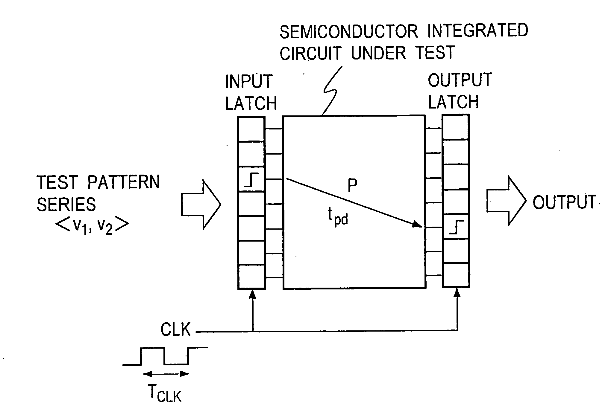
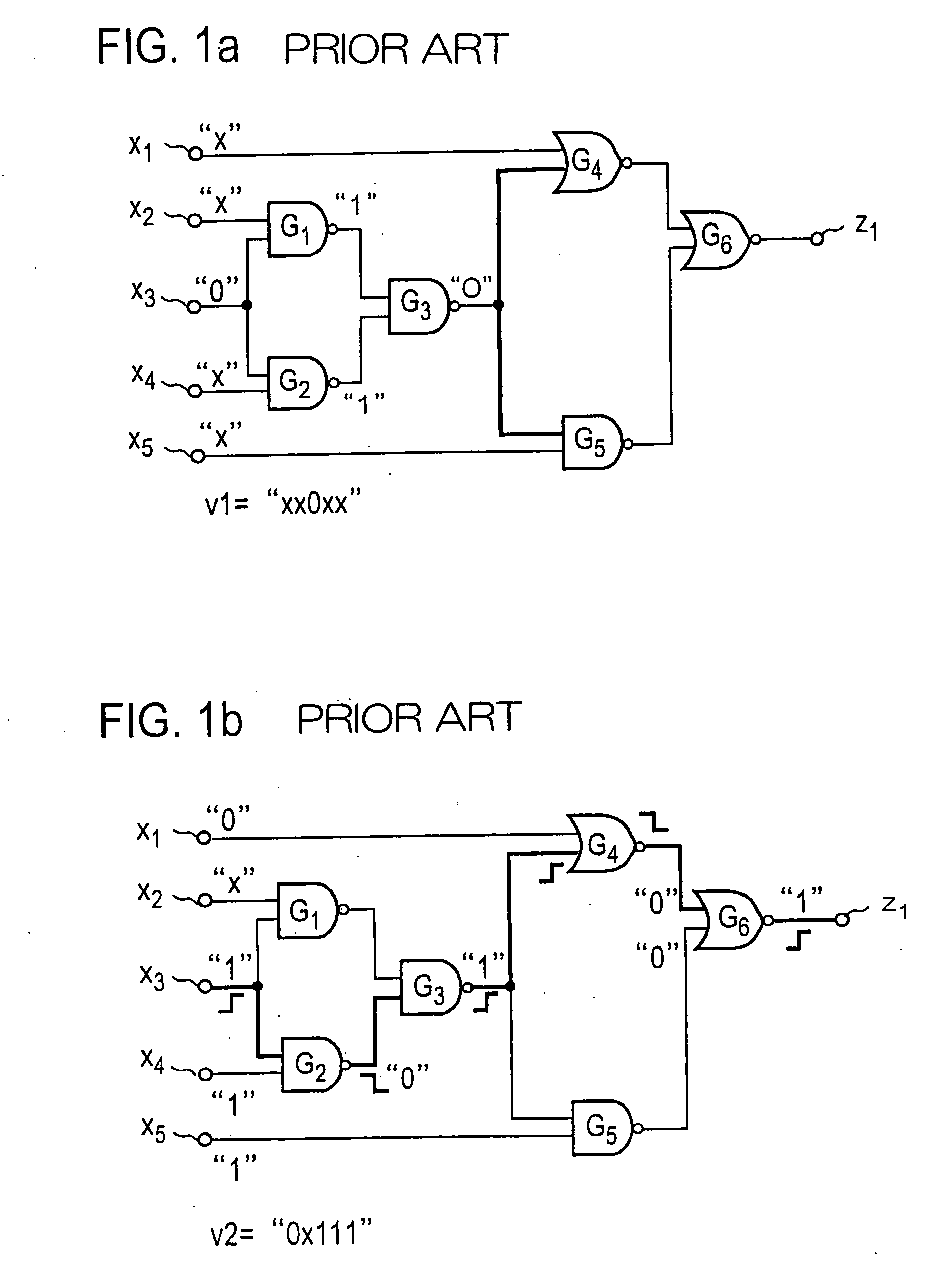
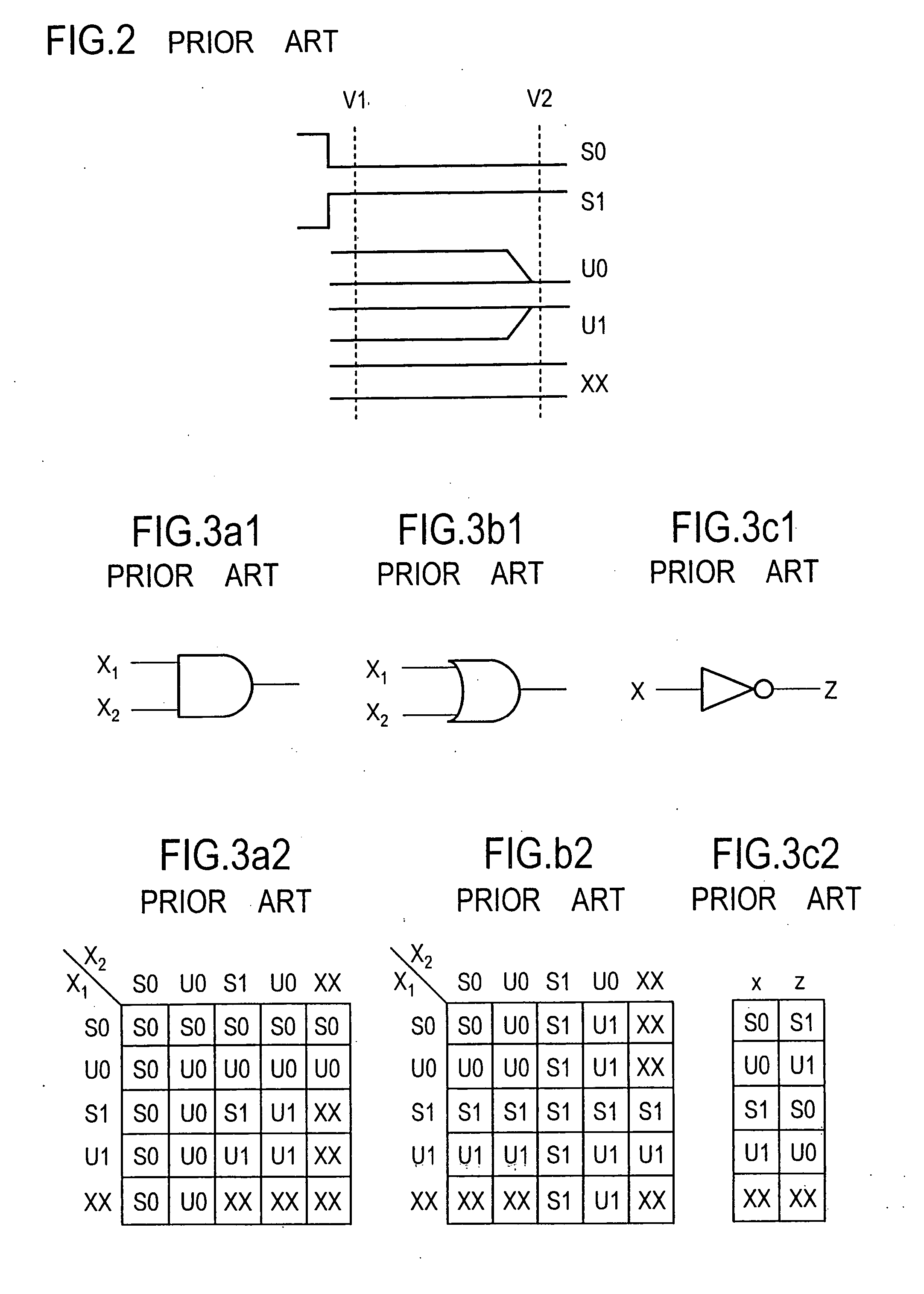
[0167]FIG. 29 shows a processing procedure for a test pattern generating method according to an embodiment of the first aspect of the present invention. Initially, at step 101, a fault list in which all faults of a semiconductor integrated circuit under test are registered is prepared. The preparation of the fault list may take place by manually enumerating slow-to-fall faults (GF) and slow-to-rise (GR) for all logic gates, for example, in the semiconductor integrated circuit under test in a sequential manner, or by automatically deriving each logic gate (each internal signal line) by an electronic computer on the basis of circuit information. At next step 102, one of the faults in the list is selected for which test patterns are to be generated. At step 103, an attempt is made to determine, by the implication operation, an initialization test pattern v1 which applies an initial value to a fault location corr...


PUM


Abstract

A test pattern sequence which is used to test a delay fault or an open fault which accompanies a delay occurring in an IC is easily and rapidly generated. A list of locations such as logic gates and signal lines within the circuit where a fault is likely to occur is prepared (101). One of the faults is selected, and an initialization test pattern v1 which establishes an initial value for activating the fault at the location of a fault is determined by the implication operation (103), and a propagation test pattern v2 which causes a stuck-at fault to be propagated to a following gate is determined by the implication operation (105). A sequence formed by v1 and v2 is registered with a test pattern list (107), and the described operations are repeated until there remains no unprocessed fault in the fault list.

Description

BACKGROUND OF THE INVENTION [0001] The invention relates a method and an apparatus for generating test patterns used in testing a semiconductor integrated circuit, and in particular, to a method and an apparatus for generating test patterns which are used to detect a gate delay fault, an open fault which gives rise to a gate delay fault, and a path delay fault with the aid of a transient power supply current signal. [0002] Test patterns for testing an abnormal delay time of a logic gate in a semiconductor integrated circuit under test (hereafter referred to as “gate delay fault”) are provided in the prior art by preparing a test pattern which initializes an output from a logic gate under test of the circuit to a signal value (initial logic value) and another test pattern which tests the logic gate under test for a stuck-at fault, or a fault that the output from the logic gate under test is fixed to the initial logic value. FIG. 1a shows an example of the semiconductor circuit under ...

Claims


Application Information

Patent Timeline
Patent Type & Authority Applications(United States)
IPC IPC(8): G01R31/28G06F11/00G01R31/3181G01R31/3183G01R31/319
CPCG01R31/2882G01R31/31813G06F11/263G01R31/318328G01R31/31917G01R31/3183
Inventor ISHIDA, MASAHIROYAMAGUCHI, TAKAHIRO
Owner ADVANTEST CORP
Why Eureka
Try Eureka