Cooling of substrate using interposer channels

a technology of interposer channel and substrate, which is applied in the direction of indirect heat exchanger, semiconductor/solid-state device details, lighting and heating apparatus, etc., can solve the problems of performance and reliability degradation of semiconductor devices, and the current methods of dissipating heat from semiconductor chips are far from optimal

Active Publication Date: 2006-03-02
GLOBALFOUNDRIES US INC
View PDF4 Cites 47 Cited by
  • Summary
  • Abstract
  • Description
  • Claims
  • Application Information

AI Technical Summary

Benefits of technology

[0024] The present invention advantageously provides a more eff...

Problems solved by technology

Insufficient transfer of heat away from a semiconductor device can result in performance and reliability degradation of the semiconductor devic...

Method used


Image

  • Cooling of substrate using interposer channels
  • Cooling of substrate using interposer channels
  • Cooling of substrate using interposer channels

Examples


Embodiment Construction

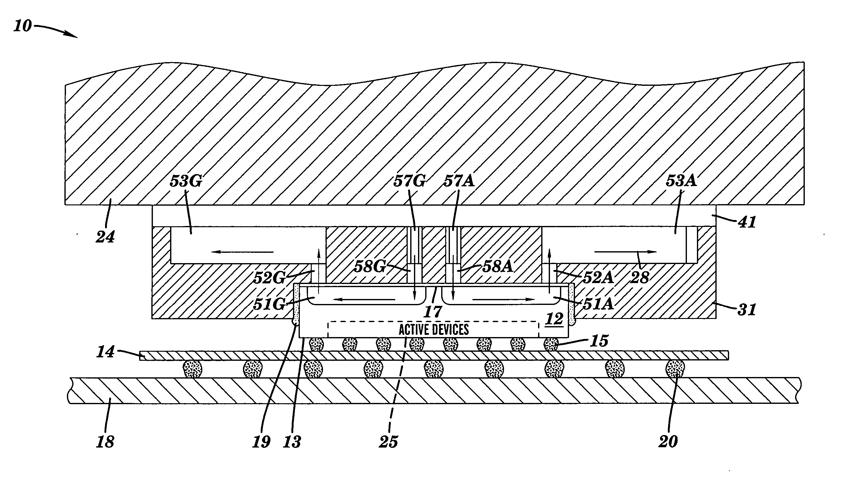
[0034]FIG. 1 illustrates a front cross-sectional view of a structure 10 comprising a semiconductor chip 12 and a interposer 31 coupled to the semiconductor chip 12, in accordance with first embodiments of the present invention. The semiconductor chip 12 comprises a semiconductor material (e.g., silicon, germanium, etc.). The semiconductor chip 12 may be underfilled with a polymer (not shown) for improved reliability.

[0035] The semiconductor chip 12 is placed in a recess in the interposer 31 with a sealant 19 placed around the semiconductor chip 12. The sealant 19, which may be thermally conductive or thermally insulative, mechanically and thermally couples the semiconductor chip 12 to the interposer 31. Although FIG. 1 shows the semiconductor chip 12 as being partially but not totally embedded within the interposer 31, the semiconductor chip 12 may alternatively be totally embedded within the interposer 31

[0036] The semiconductor chip 12 comprises a front surface 13 and an opposing...


PUM

PropertyMeasurementUnit
Molar densityaaaaaaaaaa
Structureaaaaaaaaaa
Electrical conductoraaaaaaaaaa

Abstract

A structure, and method of forming and cooling the structure. The structure may include a substrate (e.g., a semiconductor chip) having N continuous substrate channels and an interposer having N continuous interposer channels (N≧2). The N interposer channels are coupled to the N substrate channels to form M continuous loops (1≦M≦N). The M loops may transfer heat from a heat source within the substrate to the interposer and then to a heat sink thermally coupled to the interposer. The structure may include an interposer having a thermally conductive enclosure surrounding a cavity. The cavity contains a thermally conductive foam material (e.g., graphite foam). The foam material contains a serpentine channel having contiguously connected channel segments. The serpentine channel may transfer heat from a heat source within a substrate (e.g., a semiconductor chip) to the interposer and then to a heat sink thermally coupled to the interposer.

Description

BACKGROUND OF THE INVENTION [0001] 1. Technical Field [0002] The present invention relates generally to cooling a substrate, and more specifically to cooling a semiconductor chip. [0003] 2. Related Art [0004] Thermal management is relevant to the operation of semiconductors devices. The power density in semiconductor devices continues to increase as the circuit density and operating frequency increase. Thermal management includes dissipating the heat generated by a semiconductor device away from the device and allowing the generated heat to disperse to its surroundings, while maintaining the semiconductor device at as low a temperature as possible. Insufficient transfer of heat away from a semiconductor device can result in performance and reliability degradation of the semiconductor device due to an unacceptably high operating temperature. [0005] High performance semiconductor chips may have one or more “hot-spots”, which are regions of the chip having a power density that is subst...

Claims


Application Information

Patent Timeline
IPC IPC(8): H05K1/00
CPCH01L23/427H01L23/433H01L2224/16H01L2924/01019H01L2924/10253Y10T29/49128Y10T29/4913F28D15/0266Y10T29/49165Y10T29/49126Y10T29/49204H01L2924/00H01L2924/00011H01L2924/00014H01L2224/0401
Inventor LU, MINHUAMOK, LAWRENCE S.
Owner GLOBALFOUNDRIES US INC
Why Eureka
Try Eureka