Electron spectroscopic metrology system

a metrology system and electron spectroscopic technology, applied in the field of metalrology monitoring and process control, can solve the problems of less geometric resolution, affecting the accuracy of etching, etc., and achieves the effect of improving repeatability, high precision and improving accuracy

Inactive Publication Date: 2006-03-02
PENG GANG GRANT
View PDF6 Cites 12 Cited by
  • Summary
  • Abstract
  • Description
  • Claims
  • Application Information

AI Technical Summary

Problems solved by technology

The CD measurement can be taken either on the apparent feature on the image constructed from the line scanning or on the line scan itself The major limitations for the CDSEM are the less geometric resolution due to the large interaction volume, the low contrast, and most of the time, edge glowing and/or blurring.
But the nature of the CDSEM based metrology remains the same and its basic limitations are still a hurdle for metrology measurements requiring high precision and better repeatability.
nge. As the size of the semiconductor devices continues

Method used


Image

  • Electron spectroscopic metrology system
  • Electron spectroscopic metrology system
  • Electron spectroscopic metrology system

Examples


Embodiment Construction

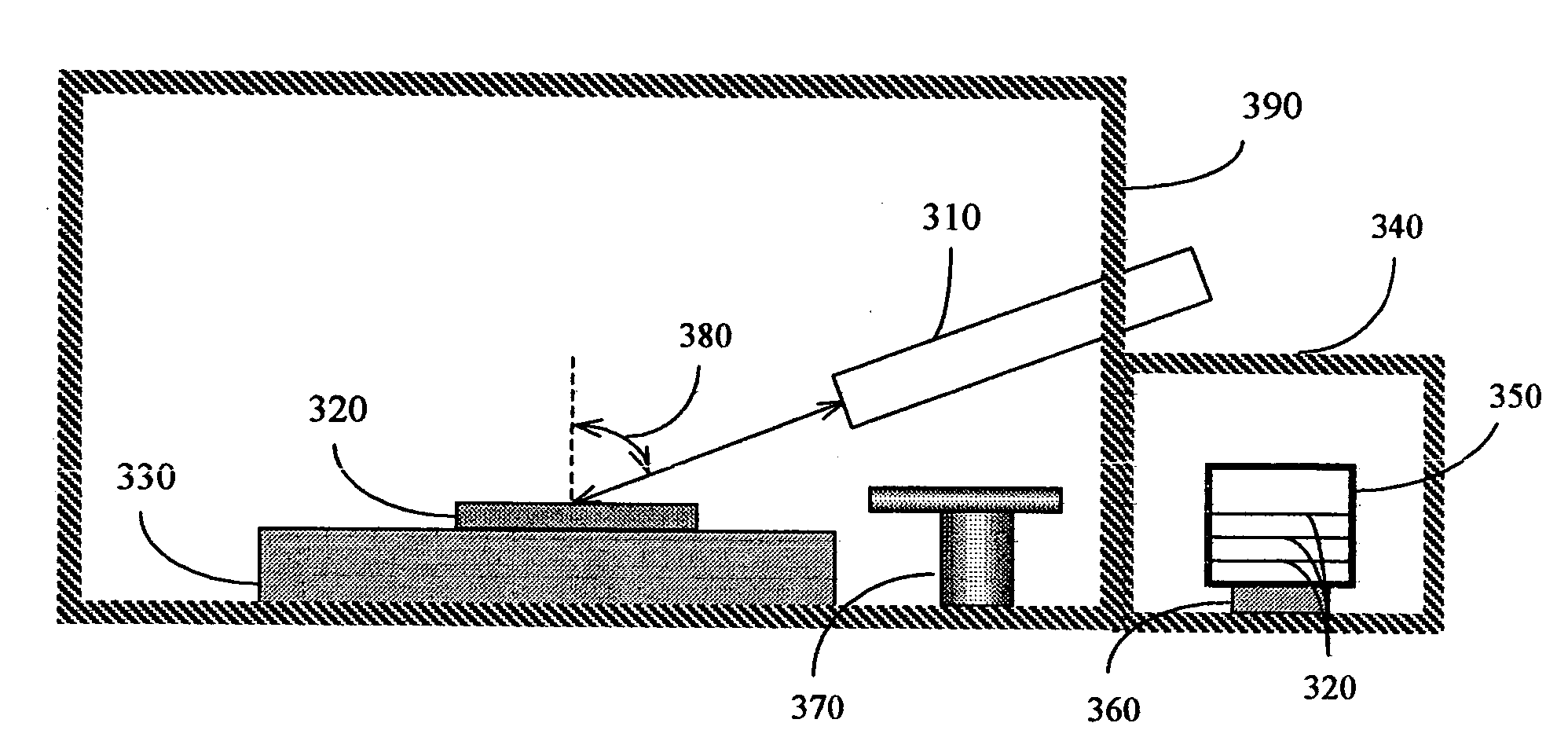
[0050] While preferred embodiments of the present invention will be described below, those skilled in the art will recognize that other hardware configurations including the electron beam from said electron source, the scan electron microscope (SEM) electron detector, the electron spectroscopic analyzer, the stage, and the substrate loading and unloading system, are capable of implementing the principles of the present invention. Thus the following description is illustrative only and not limiting.

[0051] Reference is specifically made to the drawings wherein like numbers are used to designate like members throughout.

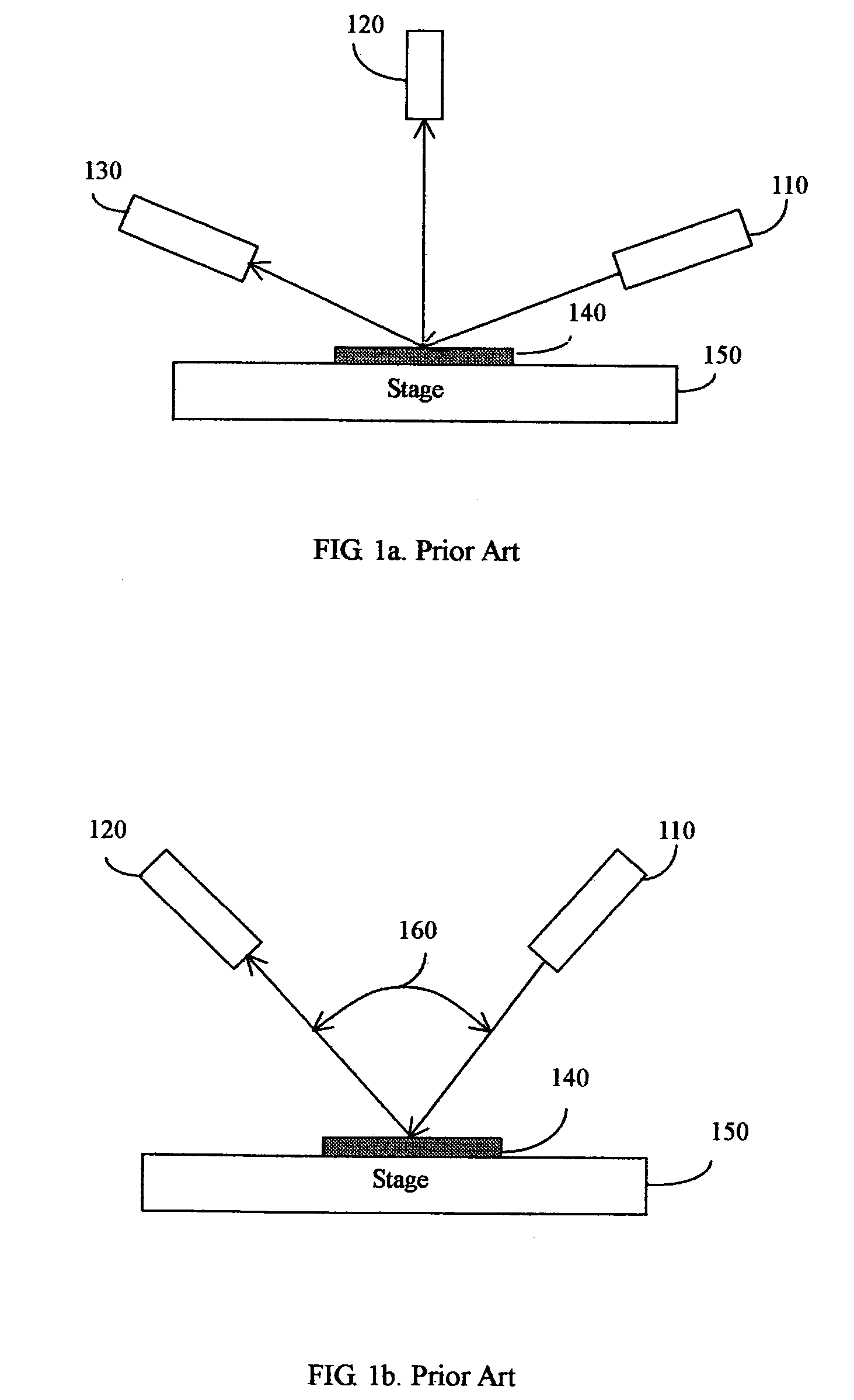
[0052] Note the followings: [0053] (1) The dimensions of all of drawings are not to scale. [0054] (2) The normal direction of the sample is equivalent to the oblique angle of zero degree. [0055] (3) The capabilities of the scan electron microscope image and pattern searching and substrate alignment of the present invention are available for all the configurations in dr...


PUM


Abstract

The present invention discloses a new electron spectroscopic metrology system using an electron beam to measure the periodic feature on a substrate. The present invention provides a measurement system for the geometry parameters of the periodic feature which is only a few repeating small elements in the measurement area. The present invention has the following advantages: (1) capable of measuring a small feature of an array of lines (line width less than a couple of ten nanometers); (2) capable of measuring a small feature of an array of via holes; (3) capable of measuring an isolated feature, with a line and patch ratio less than 1:10; (4) capable of measuring a small area, less than twenty five square micrometers; (5) no need to input detailed knowledge about the feature and its film stack; (6) simple theoretical model to derive the geometry parameters. The total simplicity of the present invention will enhance the electron spectroscopic metrology system's overall performance and productivity.

Description

BACKGROUND OF THE INVENTION [0001] (1) Field of the Invention [0002] The present invention relates to the field of metrology monitoring and process controlling of wafer fabrication processes, especially the photolithography and etching processes. [0003] (2) Prior Art [0004] The general way to monitor the wafer fabrication processes is by using a critical dimension scan electron microscope (CDSEM). The CDSEM generates an image from the electron intensity profile of the line-scan of the probe electron beam at the viewing area. Different topography and materials will have different electron deflection and second electron yields. The detector collects all the electrons available from the specimen during the line-scan, pixel by pixel, regardless of the energies of these electrons. The CD measurement can be taken either on the apparent feature on the image constructed from the line scanning or on the line scan itself The major limitations for the CDSEM are the less geometric resolution du...

Claims


Application Information

Patent Timeline
IPC IPC(8): G01N23/20H01J37/28
CPCH01J2237/2814H01J37/28
Inventor PENG, GANG GRANT
Owner PENG GANG GRANT
Why Eureka
Try Eureka