Red light-emitting device and method for preparing the same

a technology of light-emitting devices and red light, which is applied in the direction of semiconductor devices, electrical devices, nanotechnology, etc., can solve the problems of inefficient light-emitting sources, commercial optoelectronic products, and porous silicon with some major defects in application

Inactive Publication Date: 2006-03-02
INST NUCLEAR ENERGY RES ROCAEC
View PDF4 Cites 3 Cited by
  • Summary
  • Abstract
  • Description
  • Claims
  • Application Information

AI Technical Summary

Benefits of technology

[0013] The method for preparing the red light-emitting device first forms a sub-stoichiometric silica (SiOx) layer on a substrate, wherein the numerical ratio (x) of oxygen atoms to silicon atoms is smaller than 2. A thermal treating process is then performed in an oxygen-containing atmosphere at a temperature between 800 and 1300° C. for 1 to 300 minutes to transform a portion of silicon atoms in the sub-stoichiometric silica layer into a plurality of silicon nanocrystals, so that the sub-stoichiometric silica layer is transformed into a silicon dioxide layer with a plurality of silicon nanocrystals distributed therein. Another thermal treating process is performed later in a hydrogen atmosphere at a temperature between 500 and 600° C. for 1 to 120 minutes.

Problems solved by technology

At room temperature, silicon (an element of IV group in the periodic table) is an inefficient light-emitting source because it is one of the indirect band-gap materials with very low radioactive recombination rate and internal quantum efficiency of only about 10−6 to 10−7 so that silicon has not been used as a light-emitting source.
However, there are still not any commercial optoelectronic products such as the LED so far in spite of preferable result in research and development of the silicon-based LED at present.
Due to the sponge-like structure, the porous silicon has some major defects in the application to the light-emitting device.
As to the mechanical property, it is inappropriate to integrate the porous silicon with the standard semiconductor fabrication process for the frangibility of the former.
In addition, the porous silicon is highly reactive in chemical properties and is likely to react with oxygen in the atmosphere, which results in the degradation of the photoelectric property.
The degradation of the photoelectric property causes more difficulty in controlling the variation of the photoelectric properties with time.

Method used


Image

  • Red light-emitting device and method for preparing the same
  • Red light-emitting device and method for preparing the same
  • Red light-emitting device and method for preparing the same

Examples


Embodiment Construction

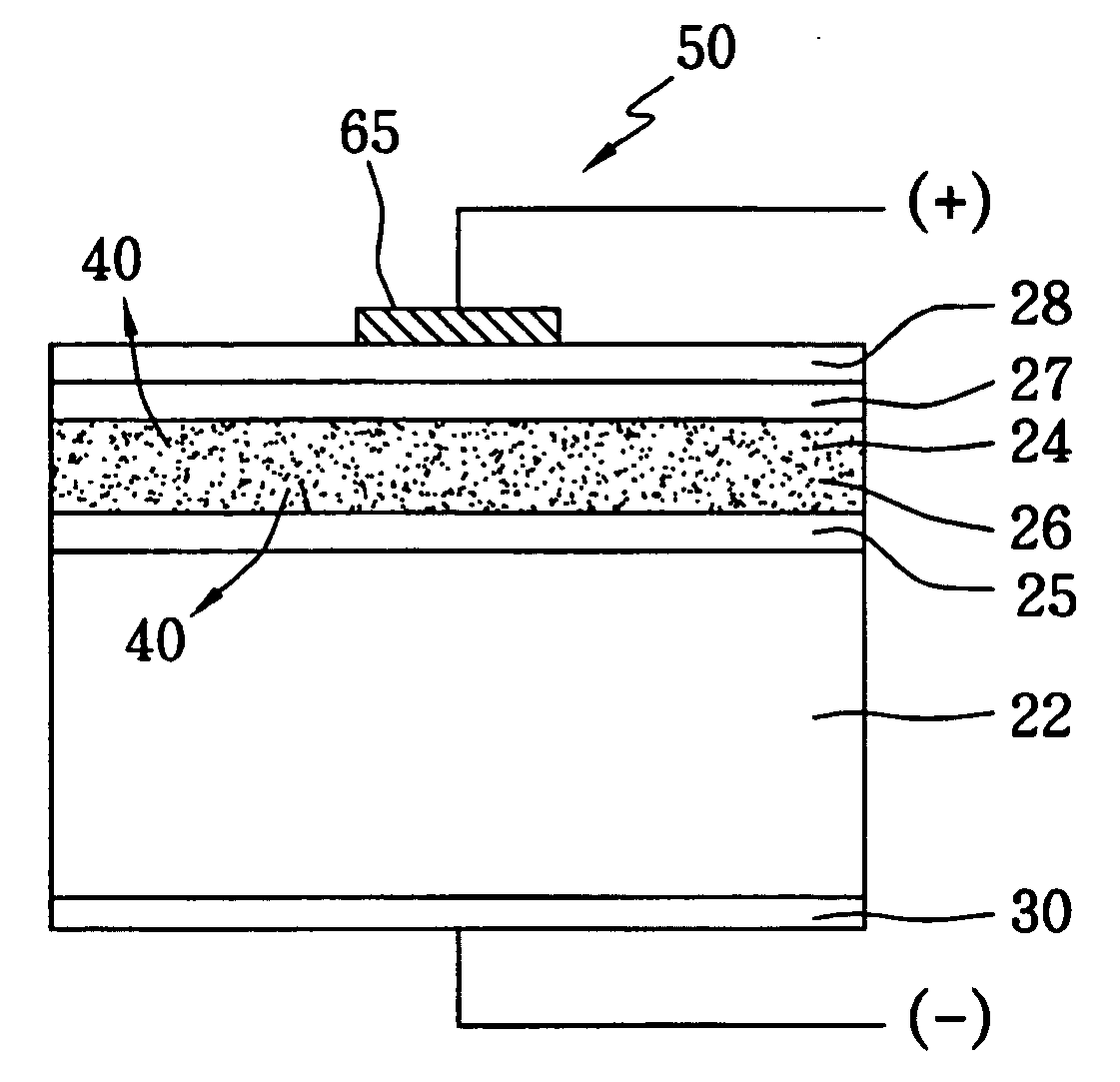
[0021] The quantum confinement effect broadens the band-gap of materials as the size of the material becomes smaller, and the nanocrystal has a distinct photoelectric property from the ordinary crystal with a larger size. Therefore, besides the well-known porous silicon, researchers also attempted to prepare the silicon-based light source by generating silicon nanocrystals (Si—NC) in a highly stable silicon dioxide layer.

[0022] The present method for preparing the Si—NC first forms a sub-stoichiometric silica (SiOx) layer with excess of silicon atoms by chemical vapor deposition (CVD), wherein the numerical ratio (x) of oxygen atoms to silicon atoms is smaller than 2. At least one high temperature annealing process is then carried out to respectively separate two different metallurgical phases (silicon and silicon dioxide), and to form the Si—NC with an order structure and the silicon dioxide with an amorphous structure simultaneously, wherein the silicon dioxide layer serves as a ...


PUM


Abstract

The present red light-emitting device includes a substrate with a first window layer, a silicon dioxide layer positioned on the first window layer, a plurality of silicon nanocrystals distributed in the silicon dioxide layer, a second window layer, a transparent conductive layer and a first ohmic contact electrode positioned in sequence on the silicon dioxide layer, and a second ohmic contact electrode positioned on the bottom surface of the substrate. The present method forms a sub-stoichiometric silica (SiOx) layer on a substrate, wherein the numerical ratio (x) of oxygen atoms to silicon atoms is smaller than 2. A thermal treating process is then performed in an oxygen atmosphere to transform the SiOx layer into a silicon dioxide layer with a plurality of silicon nanocrystals distributed therein. The thickness of the silicon dioxide layer is between 1 and 10,000 nanometers, and the diameter of the silicon nanocrystal is between 3 and 5 nanometers.

Description

RELATED U.S. APPLICATIONS [0001] Not applicable. STATEMENT REGARDING FEDERALLY SPONSORED RESEARCH OR DEVELOPMENT [0002] Not applicable. REFERENCE TO MICROFICHE APPENDIX [0003] Not applicable. FIELD OF THE INVENTION [0004] The present invention relates to a red light-emitting device and method for preparing the same, and more particularly, to a red light-emitting device with a silicon-containing active layer and method for preparing the same. BACKGROUND OF THE INVENTION [0005] There have been 36 years since Monsanto and HP et al commercialized GaAsP / GaAs red light-emitting device in 1968. Since 2000, the development of the visible light-emitting device has been primarily focusing on increasing the luminance and efficiency. After the Oil Crisis in 1973, Japan paid intention on the power consumption and successfully developed GaP red light-emitting device with low power consumption and long cycle, hence became one of suppliers of the visible light-emitting device. At present, optoelect...

Claims


Application Information

Patent Timeline
Patent Type & Authority Applications(United States)
IPC IPC(8): H01L33/00H01L33/08H01L33/34
CPCB82Y20/00H01L33/34H01L33/08
Inventor YANG, TSUN NENGLAN, SHAN MING
Owner INST NUCLEAR ENERGY RES ROCAEC
Why Eureka
Try Eureka