Nitride-based compound semiconductor light emitting device, structural unit thereof, and fabricating method thereof

Active Publication Date: 2006-03-02
SHARP FUKUYAMA LASER CO LTD
View PDF25 Cites 33 Cited by
  • Summary
  • Abstract
  • Description
  • Claims
  • Application Information

AI Technical Summary

Benefits of technology

[0014] The present invention has been made to solve the conventional technical problems described above. An object of the present invention is to improve adhesion between a bonding metal layer and an ohmic electrode as well as adhesion b

Problems solved by technology

With such a technique, however, it was difficult to uniformly heat and pressure bond the entire surface of the large-area conductive substrate to the entire surface of the nitride-based compound semiconductor layer via the ohmic electrode and the bonding metal layer.
Thus, adhesion between the conductive substrate and the nitride-based compound semiconductor layer was poor, resulting in peeling of the entire surfaces thereof.
Further, the conductive substrate would peel off from the ohmic electrode due to poor adhesion therebetween.
If the conductive substrate and the ohmic electrode are separated from each other completely, it is not possible to remove a sapphire substrate, hindering formation of a light emitting device.
If they are partially separated from each other, flow of the current from the gallium nitride-based semiconductor layer to the conductive substrate will be difficult, leading to an increase of operating voltage, thereby causing degra

Method used


Image

  • Nitride-based compound semiconductor light emitting device, structural unit thereof, and fabricating method thereof
  • Nitride-based compound semiconductor light emitting device, structural unit thereof, and fabricating method thereof
  • Nitride-based compound semiconductor light emitting device, structural unit thereof, and fabricating method thereof

Examples


example 1

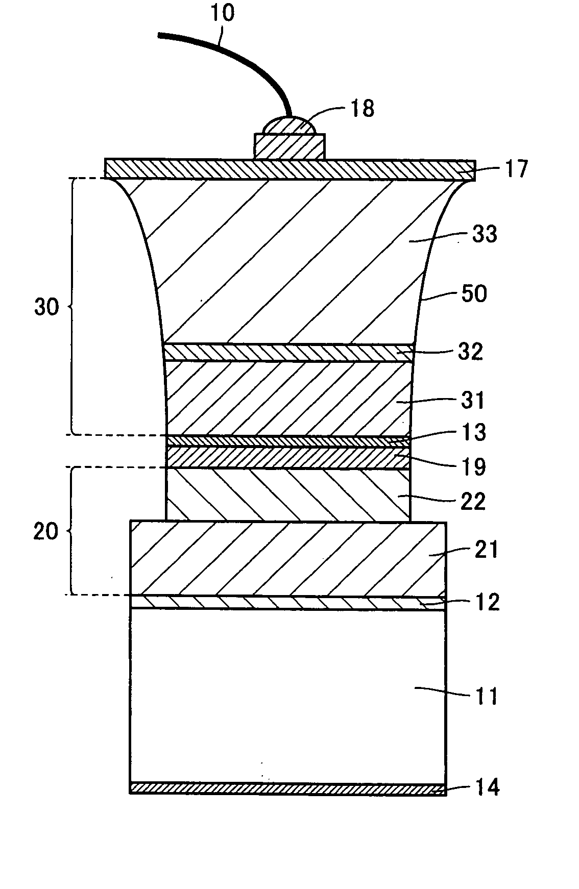
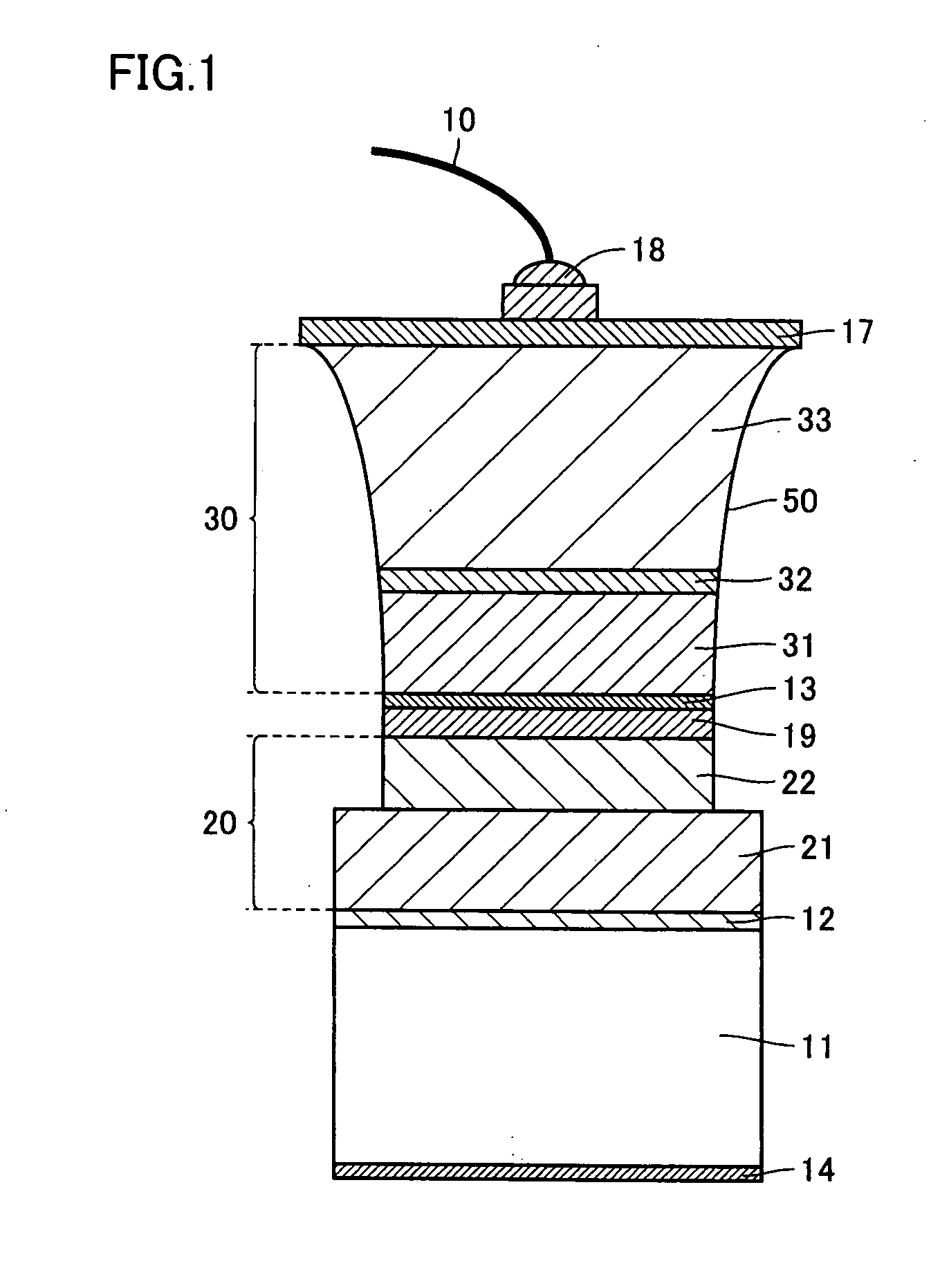
[0072] In the present example, a nitride-based compound semiconductor light emitting device as shown in FIG. 1 was formed, as will be explained in detail below.

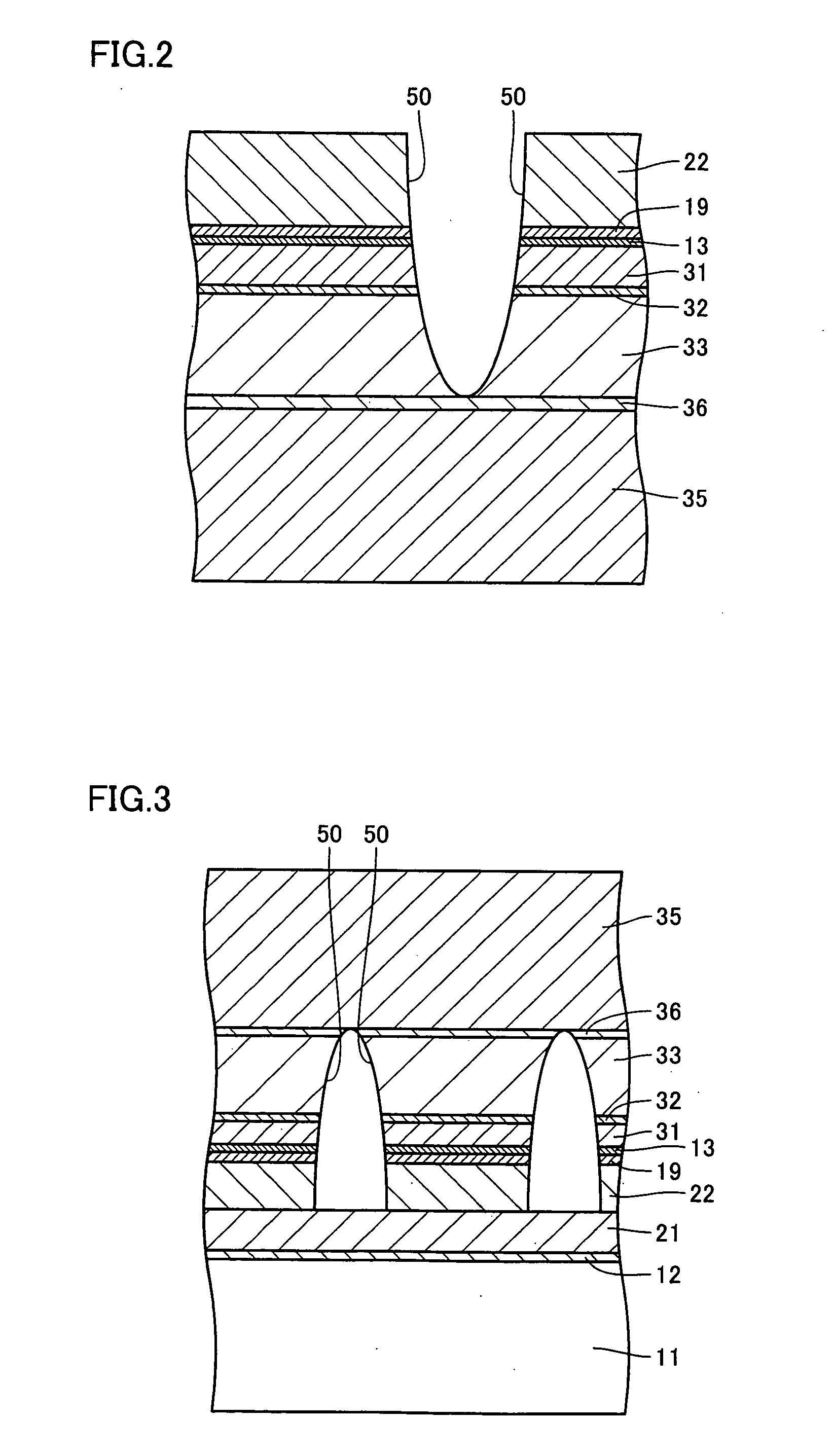
[0073] On a sapphire substrate serving as second substrate 35, a buffer layer 36 made of a GaN material, an N-type nitride-based compound semiconductor layer 33, a multi-quantum well (MQW) light emitting layer 32, and a P-type nitride-based compound semiconductor layer 31 were formed successively by MOCVD. Specifically, GaN buffer layer 36 was formed to a thickness of 20 nm, N-type nitride-based compound semiconductor layer 33 was formed to a thickness of 5 μm, MQW light emitting layer 32 was formed to a thickness of 50 nm, and P-type nitride-based compound semiconductor layer 31 was formed to a thickness of 150 nm.

[0074] Next, a concave groove portion 50 was formed in the nitride-based compound semiconductor layer formed on the sapphire substrate. RIE was employed at this time. The width of the concave groove portion was s...

example 2

[0082] In the present example, a nitride-based compound semiconductor light emitting device as shown in FIG. 6 was fabricated, as described in detail in the following.

[0083] On a sapphire substrate serving as second substrate 35, a buffer layer 36 made of a GaN material, an N-type nitride-based compound semiconductor layer 33, a MQW light emitting layer 32, and a P-type nitride-based compound semiconductor layer 31 were formed successively, by MOCVD. Specifically, on the sapphire substrate, GaN buffer layer 36 was formed to a thickness of 30 nm, N-type nitride-based compound semiconductor layer 33 was formed thereon to a thickness of 5 μm, MQW light emitting layer 32 was formed thereon to a thickness of 50 nm, and P-type nitride-based compound semiconductor layer 31 was formed thereon to a thickness of 200 nm.

[0084] Next, a concave groove portion 50 was formed in the nitride-based compound semiconductor layer on the sapphire substrate, using RIE. The concave groove portion was mad...


PUM


Abstract

A nitride-based compound semiconductor light emitting device includes a first conductive substrate, a first ohmic electrode formed on the first conductive substrate, a bonding metal layer formed on the first ohmic electrode, a second ohmic electrode formed on the bonding metal layer, and a nitride-based compound semiconductor layer formed on the second ohmic electrode. The nitride-based compound semiconductor layer includes at least a P-type layer, a light emitting layer and an N-type layer, and has a concave groove portion or a concave-shaped portion.

Description

[0001] This nonprovisional application is based on Japanese Patent Application No. 2004-255953 filed with the Japan Patent Office on Sep. 2, 2004, the entire contents of which are hereby incorporated by reference. BACKGROUND OF THE INVENTION [0002] 1. Field of the Invention [0003] The present invention relates to a nitride-based compound semiconductor light emitting device capable of emitting light in the red to ultraviolet range, a structural unit thereof, and a fabricating method thereof. More particularly, the present invention relates to a nitride-based compound semiconductor light emitting device having a conductive substrate bonded thereto and having a concave groove portion, a structural unit thereof, and a fabricating method thereof. [0004] 2. Description of the Background Art [0005] A nitride-based compound semiconductor, represented by InxGayAlzN (x+y+z=1, 0≦x<1, 0<y≦1, 0≦z<1), for example, has a large energy bandgap and high thermal stability, and allows control ...

Claims


Application Information

Patent Timeline
IPC IPC(8): H01L33/00H01L33/12H01L33/32H01L33/42
CPCH01L33/32H01L33/20H01L2224/48463
Inventor HATA, TOSHIO
Owner SHARP FUKUYAMA LASER CO LTD
Why Eureka
Try Eureka