Semiconductor device and method of manufacturing semiconductor device
a semiconductor and semiconductor technology, applied in the field of semiconductor devices, can solve problems such as variations in electrical characteristics of soi devices, and achieve the effect of reducing variations of electrical resistan
- Summary
- Abstract
- Description
- Claims
- Application Information
AI Technical Summary
Benefits of technology
Problems solved by technology
Method used
Image
Examples
first preferred embodiment
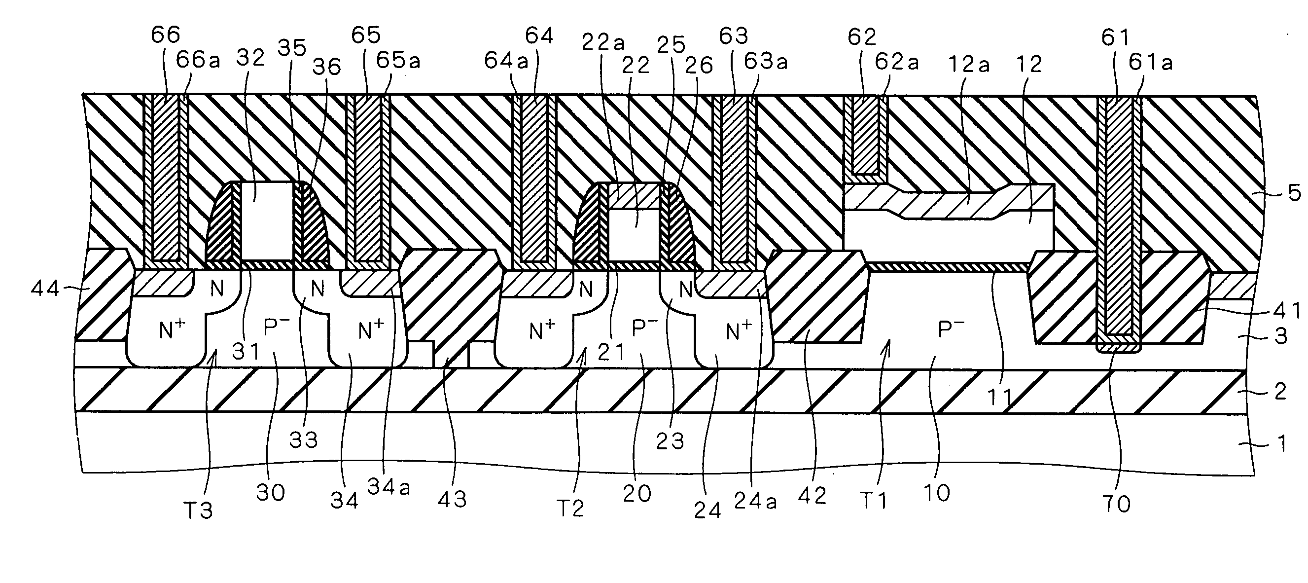
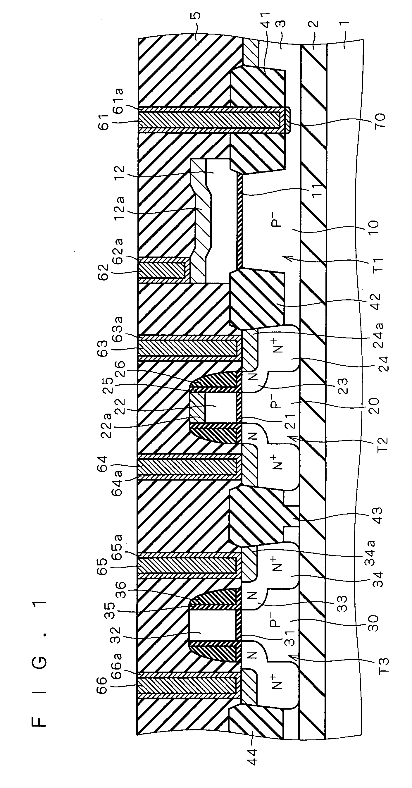
[0045]FIG. 1 shows the structure of a semiconductor device according to a first preferred embodiment of the present invention. The semiconductor device shown in FIG. 1 is an SOI device formed in an SOI substrate in which a silicon substrate 1, a buried oxide layer 2 (hereinafter referred to as “BOX layer 2”) and a P−-type silicon layer 3 (hereinafter referred to as “SOI layer 3”) are formed in this order from bottom to top.
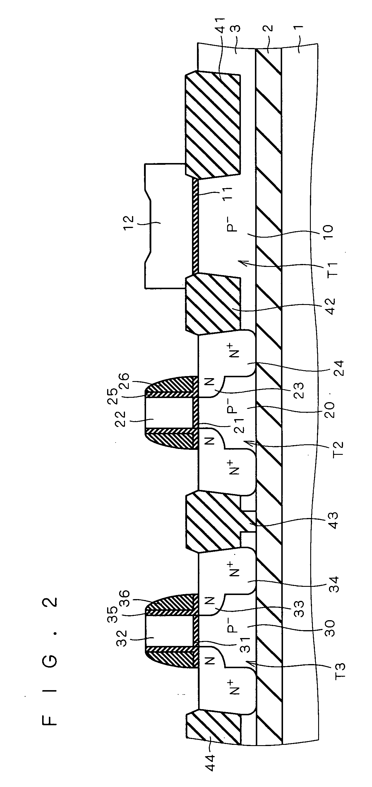
[0046] Element isolation insulating films 41, 42, 43 and 44 are formed in the upper part of the SOI layer 3 to define active regions (element forming regions) in which MOS transistors T1, T2 and T3 as semiconductor elements are formed. More specifically, the MOS transistor T1 is formed between the element isolation insulating films 41 and 42, the MOS transistor T2 is formed between the element isolation insulating films 42 and 43, and the MOS transistor T3 is formed between the element isolation insulating films 43 and 44. The element isolation insulating films 4...
second preferred embodiment
[0067]FIG. 9 shows the structure of a semiconductor device according to a second preferred embodiment of the present invention. In FIG. 9, the elements similar to those shown in FIG. 1 are designated by the same reference numerals, and will not be discussed.
[0068] In the first preferred embodiment described above, the body contact 61 penetrates the element isolation insulating film 41 to reach the SOI layer 3 thereunder. In contrast, in the second preferred embodiment, a body contact 67 is formed to be connected to the upper surface of the SOI layer 3 defined between the element isolation insulating films 41 and 45 as shown in FIG. 9. That is, in the first preferred embodiment, the body contact 61 is connected to a thin portion of the SOI layer 3 reduced in thickness as a result of the formation of the interlayer insulation film 41. In contrast, in the second preferred embodiment, the body contact 67 is connected to a thick portion of the SOI layer 3. A barrier metal 67a is formed ...
third preferred embodiment
[0076]FIG. 12 shows the structure of a semiconductor device according to a third preferred embodiment of the present invention. In FIG. 12, the elements similar to those shown in FIG. 1 are designated by the same reference numerals, and will not be discussed.
[0077] In the third preferred embodiment, a region with an impurity concentration locally lower than that of the surrounding region is provided in the vicinity of the connection between the SOI layer 3 and the body contact 61 (namely, in the vicinity of the silicide 70). In FIG. 12, this is shown as a region 73 lower in impurity concentration and high in resistance than the surrounding P− region. In the following, a P− region lower in impurity concentration than the surrounding P− region referred to as a “P− (−) region”.
[0078] A Schottky junction is formed between the SOI layer 3 and the body contact 61 without forming a P+ region at the connection between the SOI layer 3 and the body contact 61. Further, the P− (−) region 73 ...
PUM
 Abstract
Description
Claims
Application Information


