Solid state image device and camera using it

a solid-state image and image technology, applied in the field of solid-state image devices, can solve the problems of deteriorating image quality, affecting the quality of images, so as to improve the s/n proportion, improve the s/n ratio, and improve the effect of features

Inactive Publication Date: 2006-03-02
CANON KK
View PDF14 Cites 22 Cited by
  • Summary
  • Abstract
  • Description
  • Claims
  • Application Information

AI Technical Summary

Benefits of technology

[0022] The present invention is derived in view of the above described problems, and an object thereof is to provide a solid state image device with a high frame rate, that can restrain image distortion etc. from taking place in case of filming of moving pictures or rapid filming and moreover can output signals excellent in the S / N proportion, and to provide a camera using it.
[0025] In the present invention, since the frame memory unit consists of memory elements configured by capacitor means and voltage amplifying means or an operational amplifier, signals can be amplified by applying a voltage gain of 1 or more, alleviation of influence of random noise of a subsequent stage read out circuit unit 10 and improvement of S / N proportion will become feasible. In addition, an operational amplifier is excellent in features of supply-voltage rejection ratio and the like compared with other buffer means such as a source follower etc. and therefore a stable circuit can be configured. In the present invention, since the frame memory unit records outputs of all pixels, external read out of image information will become feasible during shutter and storage operations of the photoelectric conversion unit as well. According to the present invention, recording outputs of all pixels onto the frame memory, image output at a high frame rate will become feasible and external read out of image information will become feasible during shutter and storage operations of the photoelectric conversion unit as well.

Problems solved by technology

However, at this time, since the gate of the source follower Q2 gives rise to reset noise Vn to therefore result in an S / N drop, correction is necessary.
In addition, since the storage starting time of each row is different, an image will skew as shown in FIG. 14 to deteriorate an image quality.
Or in such a system that the pictured images were patched together to form a piece of image later, there was a disadvantage that seams between images were misaligned at last, etc.

Method used


Image

  • Solid state image device and camera using it
  • Solid state image device and camera using it
  • Solid state image device and camera using it

Examples


first embodiment

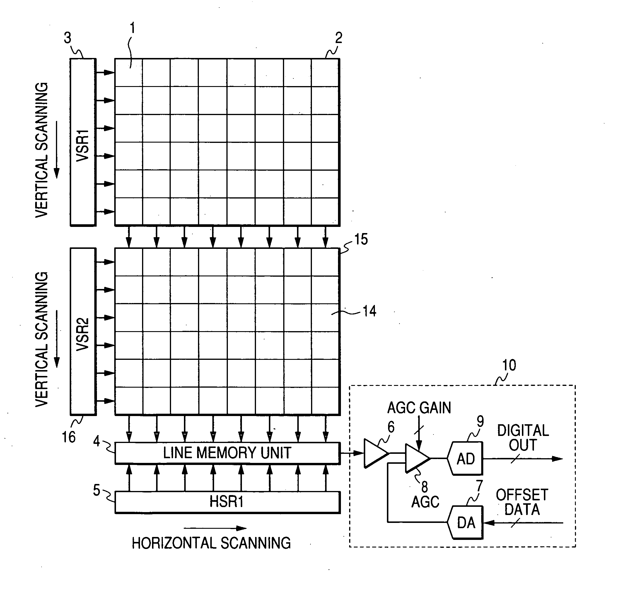
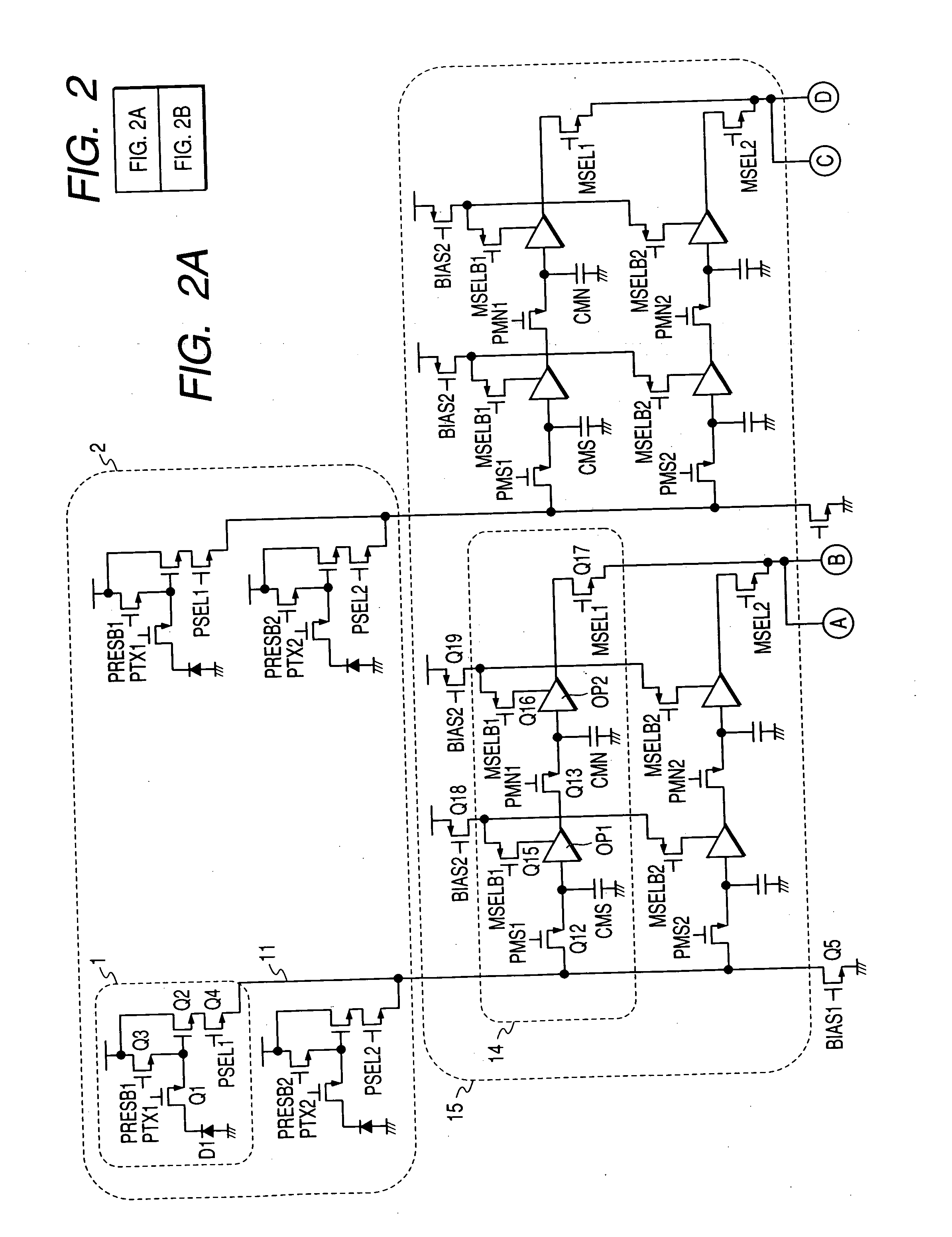
[0042]FIG. 1 is a block diagram showing a first embodiment of a solid state image device related to the present invention. Here, in FIG. 1, like reference characters designate the same parts in FIG. 10 and descriptions thereon will be omitted. FIG. 1 is different from FIG. 10 in that a frame memory unit 15 with memory element 14 being two-dimensionally arranged equivalent to the photoelectric conversion unit 2 and a second vertical shift register 16 (VSR2) to drive the frame memory unit 15 are present behind the photoelectric conversion unit 2. Here, the arrangement of the pixels and the memory elements is 6 rows by 8 columns, but the arrangement will not be limited thereto but is optional.

[0043] In addition, each pixel of the photoelectric conversion unit 2 corresponds one-to-one with each memory element of the frame memory 15 so that the output of each row of the photoelectric conversion unit 2 selected by the first vertical shift register 3 is respectively stored in the memory e...

second embodiment

[0063]FIG. 5 is a block diagram showing a second embodiment of the present invention. Here, in FIG. 5, like reference characters designate the same parts in FIG. 1 and descriptions thereon will be omitted. FIG. 5 is different from FIG. 1 in that a photoelectric conversion unit 2 and a frame memory unit 15 respectively have second vertical shift registers 17 and 18. Moreover, FIG. 5 is different from FIG. 1 in that a second line memory 19, a horizontal shift register 20 and operational amplifiers 6 are present and outputs of the first and the second operational amplifiers 6 are selected by a switch 21 and inputted to a gain control amplifier 8. Here, the arrangement of the pixels and the memory elements is 6 rows by 8 columns, but the arrangement will not be limited thereto but is optional.

[0064] In addition, these two units each of the vertical shift registers 3, 17 and 16, 18 are driven by shift pulses with 180-degree phase discrepancy and operate so as to select the photoelectric...

third embodiment

[0075]FIG. 9 is a block diagram showing an embodiment of a still camera with a solid state image device of the present invention as described above. In FIG. 9, reference numeral 101 denotes a barrier that combines protection of a lens and a main switch, reference numeral 102 denotes a lens of forming an optical image of an object into a solid state image device 104, reference numeral 103 denotes a diaphragm of varying a light quantity that has passed the lens 102 and reference numeral 104 denotes a solid state image device for taking in an object that has undergone image forming with the lens 102 as an image signal. The solid state image device 104 corresponds with the solid state image device of the present invention described above.

[0076] Reference numeral 106 denotes an A / D converter of implementing digital-analogue conversion on the image signal outputted from the solid state image device 104. Reference numeral 107 denotes a signal processing unit of implementing respective kin...


PUM


Abstract

A solid state image device with a high frame rate, that can restrain image distortion etc. from taking place in case of filming of moving pictures or rapid filming and moreover can output signals excellent in the S / N proportion in a stable fashion, and a camera using it is provided. A frame memory apparatus having a plurality of memories respectively corresponding with respective pixels of a photoelectric conversion apparatus and an apparatus of recording signals of respective pixels of the photoelectric conversion apparatus into the memory elements of the frame memory apparatus are included. The memory element is configured at least by a sample hold circuit, the sample hold circuit has a capacitor apparatus and an impedance conversion apparatus and the impedance conversion apparatus is configured by an operational amplifier.

Description

BACKGROUND OF THE INVENTION [0001] 1. Field of the Invention [0002] The present invention relates to a solid state image device, in particular to a solid state image device suitable to an image system of acquiring a moving picture or images at a high frame rate to synthesize them to form an image and a camera using it. [0003] 2. Related Background Art [0004]FIG. 10 is a block diagram showing a prior art solid state image device. This has been disclosed, for example, in Japanese Patent Application Laid-Open No. H11-196332 being a Japanese patent. The solid state image device in FIG. 10 has a pixel 1 which converts an optical signal to an electric signal, a photoelectric converter 2 with a plurality of pixels 1 being arranged two-dimensionally, a vertical shift register 3 (VSR1) which selects the two-dimensionally arranged pixels sequentially on a row-by-row basis in the vertical direction. Moreover, the solid state image device in FIG. 10 has a line memory unit 4 that retains each pi...

Claims


Application Information

Patent Timeline
Patent Type & Authority Applications(United States)
IPC IPC(8): H04N1/04H04N5/335H04N5/341H04N5/353H04N5/374H04N101/00
CPCH04N3/1543H04N3/1518H04N25/42H04N25/616H04N25/75
Inventor SATO, TOSHIAKISAITO, KAZUHIRO
Owner CANON KK
Why Eureka
Try Eureka