Optical switch and optical waveform monitoring device utilizing optical switch

a monitoring device and optical switch technology, applied in the direction of optics, optical light guides, instruments, etc., can solve the problems of limited operation speed, signal or control signal has the same problem in terms of operation speed, and high-speed signal limit, and achieve the effect of high switching efficiency

Inactive Publication Date: 2006-03-02
FUJITSU LTD
View PDF5 Cites 47 Cited by
  • Summary
  • Abstract
  • Description
  • Claims
  • Application Information

AI Technical Summary

Benefits of technology

[0019] It is an object of the present invention to provide a technique for switching optical signal in high switching efficiency.

Problems solved by technology

However, it requires dedicated electronic circuitry for every bit rate to be supported, and has a high-speed signal limit due to a limit in the operation speed of electronics.
The above-mentioned technology (2) using electrical signals as driving signals or control signals has the same problem in terms of operation speed.
The above-mentioned technology (3) does not have a limited operation speed because it does not employ electrical signals, however adoption of high-speed signals more than 160 Gbps leads to issues such as losses of 10-30 dB on switching and a narrow range of wavelengths that can be switched.
Decrease in switching efficiency causes a decrease in the optical S / N ratio and degradation of signal quality.
Further, narrow operating bandwidth requires optical switches for each signal wavelength.

Method used


Image

  • Optical switch and optical waveform monitoring device utilizing optical switch
  • Optical switch and optical waveform monitoring device utilizing optical switch
  • Optical switch and optical waveform monitoring device utilizing optical switch

Examples


embodiment 1

(Embodiment 1)

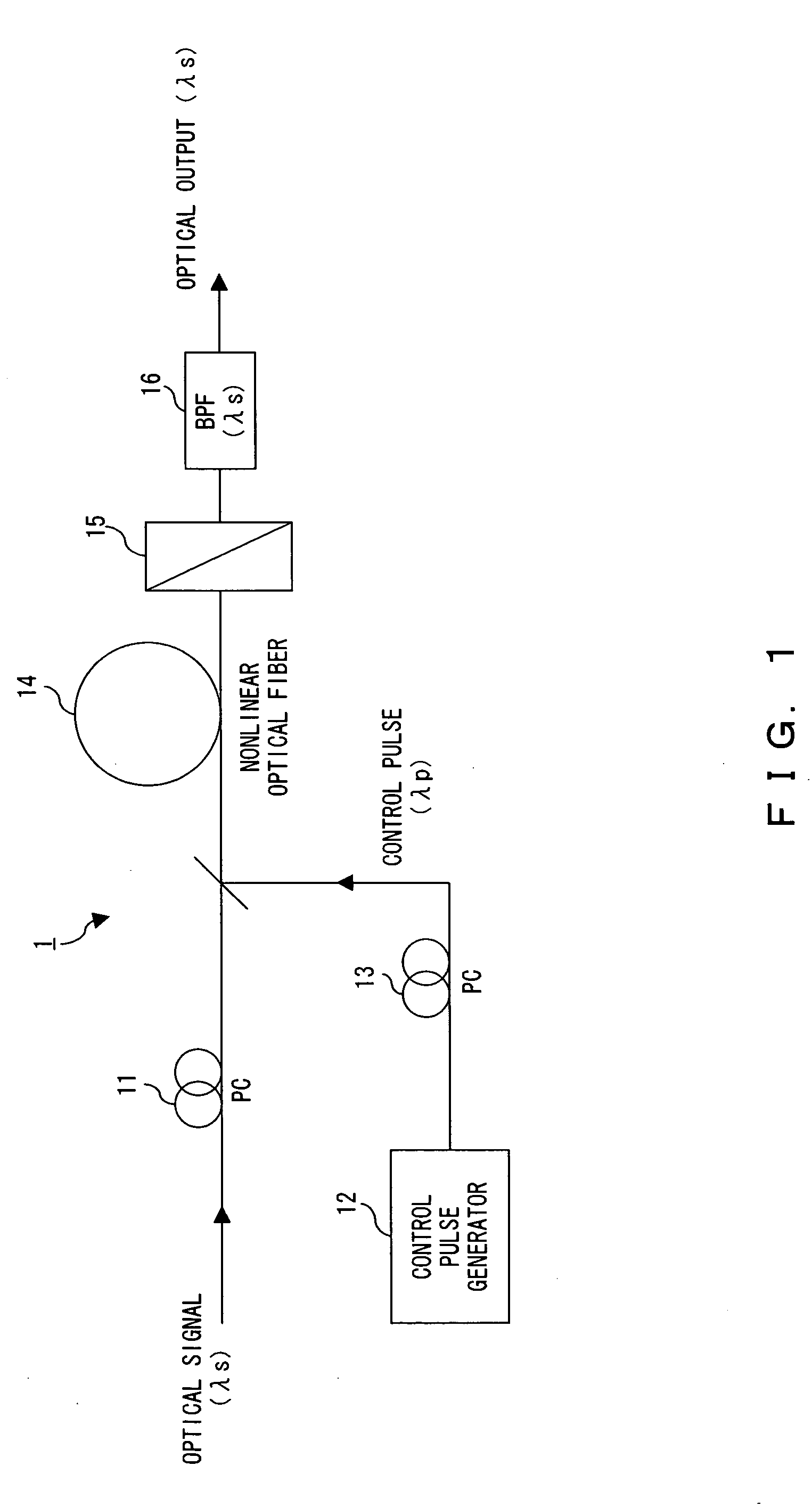
[0156]FIG. 28 is a diagram describing a configuration of the system for testing characteristics of the optical switch of the present invention. The testing environment is provided below.

[0157] Highly nonlinear fiber (HNLF) is equivalent to the nonlinear optical fiber 14 in FIG. 1. It is 20 m long and has a third-order nonlinear coefficient γ of 20.4 W−1km−1, a zero dispersion wavelength λ0 of 1579 nm, and a dispersion slope of 0.03 ps / nm2 / km. A first Mode-locked fiber laser (MLFL1) generates a series of pulses with a repetition rate of 10 GHz at a wavelength λs in the C-band. The series of optical pulses is modulated by an LiNbO3 intensity modulator (LN, 10 Gbps, PRBS:223−1), the modulated signal is multiplexed by optical time-division multiplexing to generate a data signal Es of 160˜640 Gbps. With control pulse Ep generated by a second mode-locked fiber laser (MLFL2), the data signal Es is fed to the highly nonlinear fiber HNLF. The wavelength of the control pulse Ep...

embodiment 2

(Embodiment 2)

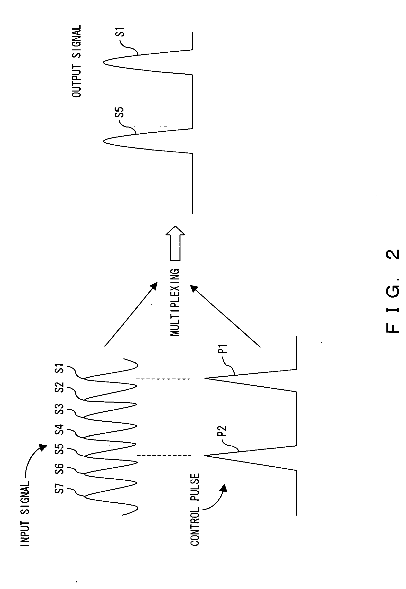
[0161] Experimental data for optical demultiplexer, which splits a 10 Gbps signal from an optical time-division multiplexed signals Es of 160 Gbps, 320 Gbps, and 640 Gbps is provided below. The pulse width of signal Es at 160 Gbps is 1.6 ps, that of signal Es at 320 Gbps is 0.75 ps, and that of signal Es at 640 Gbps is 0.65 ps. The pulse width of the control pulse Ep is 0.9 ps.

[0162]FIG. 31 is a graph showing measured values of BER (Bit Error Rate) when the reception power PR of the split signal is changed. The average power of the control pulse is +21.8 dBm (equivalent to peak power=15 W). The average power of the input signal Es of 160 Gbps to the optical switch is −5 dBm.

[0163] At 160 Gbps, bit error rates for each signal wavelength λs=1535 nm, 1540 nm, 1550 nm, and 1560 nm are measured. As a result, error-free operation (BER=10−9) with a power penalty of less than 0.2 dB is achieved for all wavelengths in the C-band. Signals with 320 Gbps and 640 Gbps, error-free...

embodiment 3

(Embodiment 3)

[0164] Signal waveforms observed with an oscilloscope after sampling utilizing the optical switch of the present invention are shown. FIG. 32A through FIG. 32E show the observed eye diagrams when the pulse width conditions are the same as explained in Embodiment 2. The sampling rate is 311 MHz. Excellent eye diagrams are obtained throughout the range of 160 through 640 Gbps. Such fine time resolution is a great contribution to the implementation of optical sampling with high contrast over the entire range of the C-band.

[0165] The following document provides descriptions of the embodiments 1˜3 explained above.

[0166] S. Watanabe, et al. “Novel Fiber Kerr-Switch with Parametric Gain: Demonstration of Optical Demultiplexing and Sampling up to 640 Gb / s”, 30th European Conference on Optical Communication (ECOC 2004), Stockholm, Sweden, September 2004, Post-deadline paper Th4.1.6, pp 12-13.


PUM


Abstract

The polarization direction of a signal is rotated by a polarization controller so as to be orthogonal to the main axis of a polarizer. A control pulse generator generates control pulses from control source with a wavelength which is different from the wavelength of the signal. The signal and the control pulse are input to a nonlinear optical fiber. In the nonlinear optical fiber, the signal, during the time period in which the signal and the control pulse coincide, has its polarization direction rotated by cross phase modulation, and is amplified by optical parametric amplification. The signal, during the time period in which the signal and the control pulse coincide, passes through the polarizer.

Description

BACKGROUND OF THE INVENTION [0001] 1. Field of the Invention [0002] The present invention relates to technology for extraction of part of an optical signal, more specifically to a method of extracting time-division-multiplexed optical signals with a series of light pulses or a component of the signals, to an optical switch that utilizes the method and to an optical sampling oscilloscope that utilizes the optical switch. [0003] 2. Description of the Related Art [0004] Increase in data volume and the need for long-distance communication in recent years have promoted a wide spread of devices and systems utilizing optical technology. A part of this technology, the optical switch, which extracts a part of an optical signal consisting of a series of pulses of light, is under research and development as a core element. The following methods are known as conventional technology for switching optical signals consisting of a series of pulses of light: [0005] (1) A technology, which first conv...

Claims


Application Information

Patent Timeline
Patent Type & Authority Applications(United States)
IPC IPC(8): G02B6/26G02B6/00
CPCG02F1/3515H04J14/08G02F1/39G02F1/3519
Inventor WATANABE, SHIGEKI
Owner FUJITSU LTD
Why Eureka
Try Eureka