Top anti-reflective coating composition and method for pattern formation of semiconductor device using the same

Active Publication Date: 2006-03-02
SK HYNIX INC
View PDF10 Cites 13 Cited by
  • Summary
  • Abstract
  • Description
  • Claims
  • Application Information

AI Technical Summary

Benefits of technology

[0011] A top anti-reflective coating composition is disclosed which is water insoluble and, therefore, can be used in immersion lithography. Other desired properties of a top anti-reflective coating composition include its ability to prevent the multiple interference of light in

Problems solved by technology

Several issues arise from the use of EUV and F2 lasers as light sources.
However, high-quality CaF2 is difficult to produce on an industrial scale within a short time.
Also, since soft pellicles are likely to be deformed upon exposure to light at 157 nm, the lifetime of the light source is short; hard pellicles incur considerable production costs, and are difficult to produce on a commercial scale due to the nature of light refraction.
Suitable light sources, exposure equipment and masks are required for EUV laser use, making their application impractical.
A problem encountered with the fabrication of a sub-50 nm semiconductor device is that alteration of the critical dimension (CD) of a photoresist pattern inevitably occurs during the process fo

Method used


Image

  • Top anti-reflective coating composition and method for pattern formation of semiconductor device using the same
  • Top anti-reflective coating composition and method for pattern formation of semiconductor device using the same
  • Top anti-reflective coating composition and method for pattern formation of semiconductor device using the same

Examples


example 1

Preparation of a Top Anti-Reflective Coating Composition and Pattern Formation

[0050] 2.5 g of poly(t-butylacrylate-acrylic acid-3-hydroxypropylmethacrylate) and 0.15 g of triphenylsulfonium perfluorooctanesulfonate (Formula 5) were dissolved in 100 g of n-butanol to create a top anti-reflective coating composition for immersion lithography.

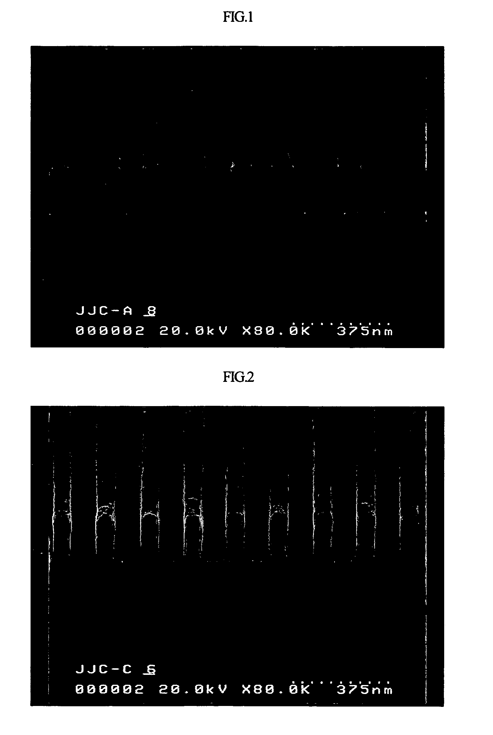
[0051] A photosensitizer (AR1221J, JSR) was coated to a thickness of 220 nm on a wafer, and baked at 130° C. for 90 seconds. The top anti-reflective coating composition was coated at 3,000 rpm on the photosensitizer, and baked at 90° C. for 60 seconds. After exposing the wafer to light using ArF exposure equipment, the exposed wafer was baked at 130° C. for 90 seconds and developed to form a pattern. An image of the pattern is shown in FIG. 2. This image indicates that the pattern was vertically formed when compared to the pattern formed in Comparative Example 1 (see FIG. 1).

example 2

Preparation of a Top Anti-Reflective Coating Composition and Pattern Formation

[0054] A top anti-reflective coating composition was prepared in the same manner as in Example 1, except that poly(t-butylacrylate-acrylic acid-N-isopropylacrylamide) was used as a top anti-reflective coating polymer. Further, a pattern was formed using the top anti-reflective coating composition in the same manner as in Example 1.

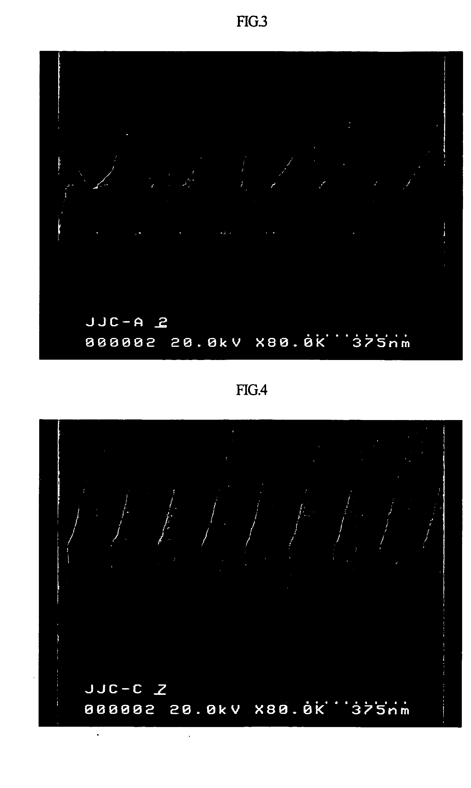
[0055] An image of the pattern thus formed is shown in FIG. 4. This image indicates that the pattern was vertically formed when compared to the pattern formed in Comparative Example 2 (see FIG. 3).

example 3

Preparation of a Top Anti-Reflective Coating Composition and Pattern Formation

[0058] A top anti-reflective coating composition was prepared in the same manner as in Example 1, except that poly(t-butylacrylate-acrylic acid-2-hydroxyethylmethacrylate) was used as a top anti-reflective coating polymer. Further, a pattern was formed using the top anti-reflective coating composition in the same manner as in Example 1.

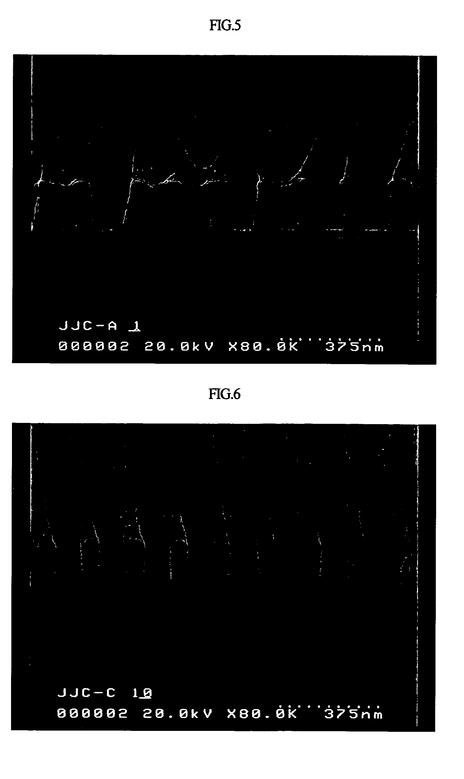
[0059] An image of the pattern thus formed is shown in FIG. 6. This image indicates that the pattern was vertically formed when compared to the pattern formed in Comparative Example 3 (see FIG. 5).

[0060] As apparent from the above description, the top anti-reflective coatings formed using the anti-reflective coating compositions of the disclosure allow for better-quality results from immersion lithography over those compositions and coating previously disclosed. Since the top anti-reflective coating has a light transmission of 96% or higher, it is transparent to a light s...


PUM

PropertyMeasurementUnit
Temperatureaaaaaaaaaa
Fractionaaaaaaaaaa

Abstract

Disclosed herein is a top anti-reflective coating composition which comprises a photoacid generator represented by Formula 1 below.
wherein n is between 7 and 25. Since the top anti-reflective coating composition dissolves a portion of a photoacid generator present at the top of an underlying photosensitizer, particularly, upon formation of a top anti-reflective coating, it can prevent the top from being formed into a thick section. Therefore, the use of the anti-reflective coating composition enables the formation of a vertical pattern on a semiconductor device.

Description

BACKGROUND [0001] 1. Technical Field [0002] The disclosure relates to an anti-reflective coating composition used in photolithography, which is a fabrication process for semiconductor devices, and a method for forming a pattern of a semiconductor device using the anti-reflective coating composition. More specifically, the disclosure relates to a top anti-reflective coating composition usable in immersion lithography for the fabrication of sub-50 nm semiconductor devices, and a method for forming a pattern of a semiconductor device using the top anti-reflective coating composition. [0003] 2. Description of the Related Art [0004] Photolithography is a process for the transfer of a semiconductor circuit pattern formed on a photomask to a wafer, and is one of the most important processes in determining the fineness and integration density of circuits in the fabrication of semiconductor devices. [0005] In recent years, as the integration density of semiconductor devices has increased, ne...

Claims


Application Information

Patent Timeline
IPC IPC(8): G03C1/76
CPCC08K5/42C09D133/06G03F7/0045H01L21/312G03F7/0392G03F7/091G03F7/095G03F7/0046H01L21/02282H01L21/02118C08L33/06H01L21/02107
Inventor JUNG, JAE CHANGBOK, CHEOL KYUKIM, SAM YOUNGLIM, CHANG MOONMOON, SEUNG CHAN
Owner SK HYNIX INC
Why Eureka
Try Eureka