Recessed gate dielectric antifuse

Active Publication Date: 2006-03-02
MICRON TECH INC
View PDF29 Cites 58 Cited by
  • Summary
  • Abstract
  • Description
  • Claims
  • Application Information

AI Technical Summary

Benefits of technology

[0006] It is against the above mentioned background, that the present invention provides a number of unobvious advantages and advances over the prior art. In particular, the present invention discloses a recessed dielectric antifuse device and method of formation thereof. The antifuse device includes a substrate and laterally spaced source and drain regions formed in the substrate. A recess is formed between the source and drain regions. A ga

Problems solved by technology

When the MOSFET is stressed beyond a critical electrical field by applying suffic

Method used


Image

  • Recessed gate dielectric antifuse
  • Recessed gate dielectric antifuse
  • Recessed gate dielectric antifuse

Examples


Example

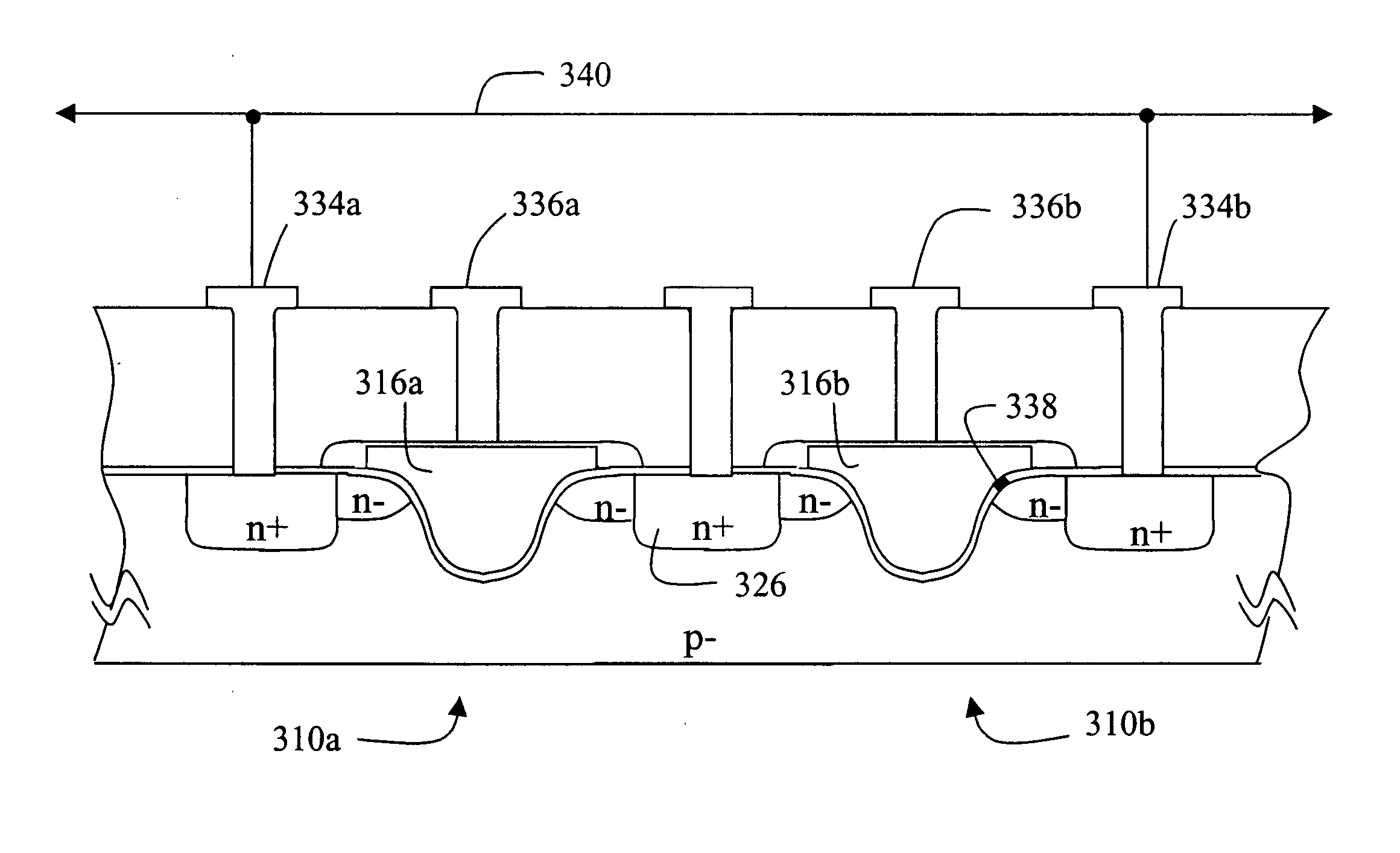
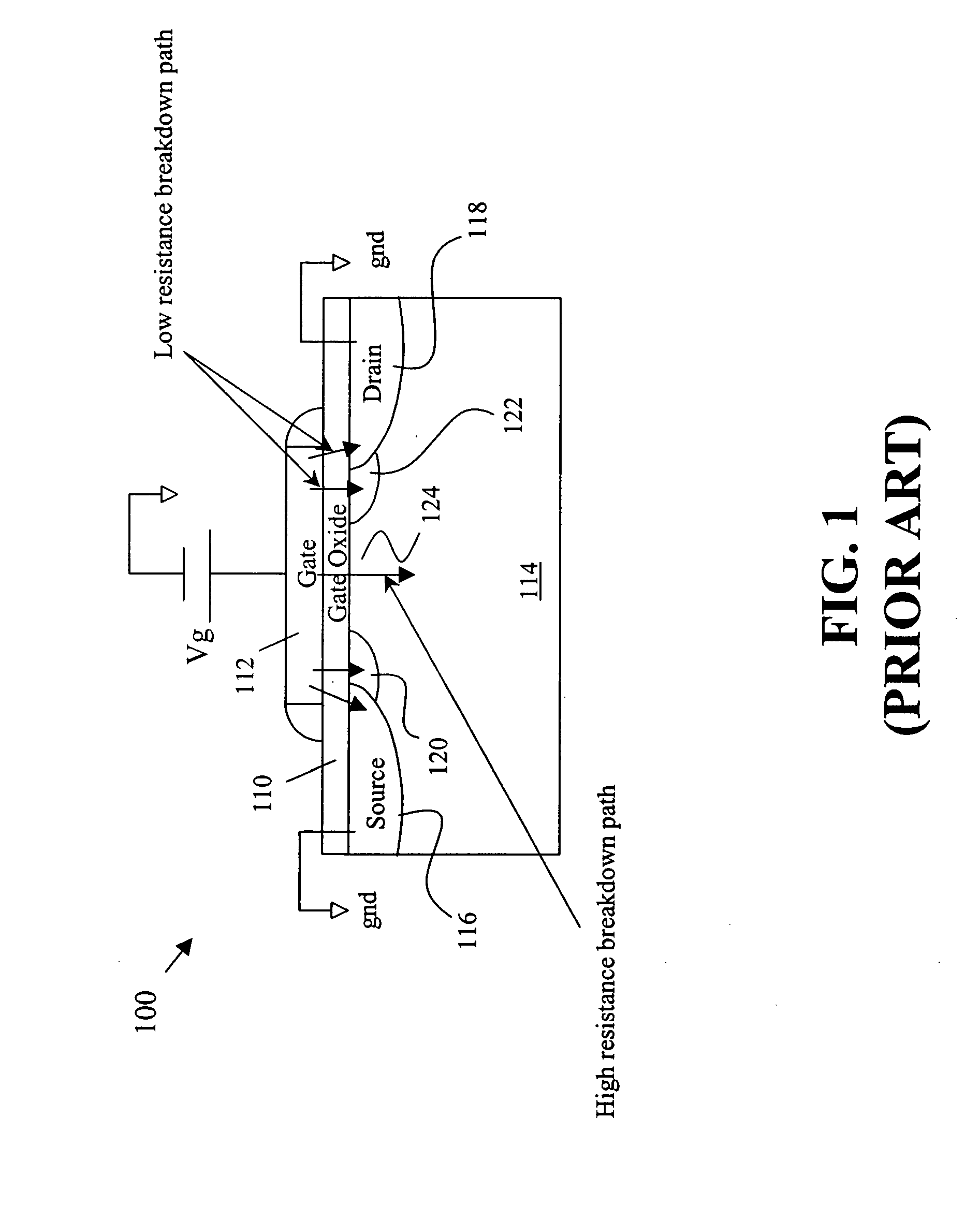
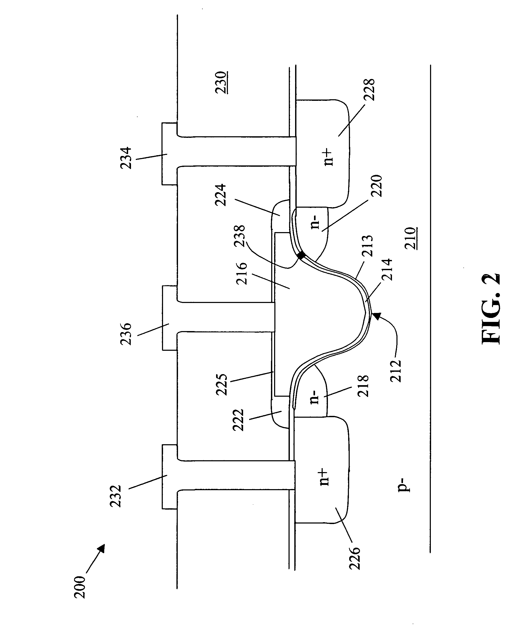
[0012] The invention disclosed herein is directed to a recessed gate oxide antifuse and a method of fabricating the recessed gate oxide antifuse structure. The drawing figures illustrate a partially completed integrated circuit device. In the following description, numerous details are set forth in order to provide a thorough understanding of the present invention. It will be appreciated by one skilled in the art that variations of these specific details are possible while still achieving the results of the present invention.

[0013] Additionally, well-known processing steps are not described in detail in order not to unnecessarily obscure the present invention. For the sake of brevity, conventional electronics, semiconductor manufacturing, memory technologies and other functional aspects of the devices (and components of the individual operating components of the devices) may not be described in detail herein. Furthermore, for purposes of brevity, the invention is frequently describ...


PUM


Abstract

A recessed dielectric antifuse device includes a substrate and laterally spaced source and drain regions formed in the substrate. A recess is formed between the source and drain regions. A gate and gate oxide are formed in the recess and lightly doped source and drain extension regions contiguous with the laterally spaced source and drain regions are optionally formed adjacent the recess. Programming of the recessed dielectric antifuse is performed by application of power to the gate and at least one of the source region and the drain region to breakdown the dielectric, which minimizes resistance between the gate and the channel.

Description

BACKGROUND OF THE INVENTION [0001] The present invention relates to a semiconductor device, and more particularly, to a recessed gate dielectric antifuse. [0002] A conventional Metal Oxide Semiconductor Field Effect Transistor (MOSFET) comprises a doped polysilicon gate, a channel conduction region, and source / drain regions formed by diffusion of dopants in the silicon substrate. The channel region separates the source from the drain in the lateral direction. A substantially planar layer of a dielectric material that prevents electrical current flow separates the polysilicon gate from the channel. The substantially planar dielectric material separating the polysilicon gate from the channel region, henceforth referred to as the gate oxide, usually consists of the thermally grown silicon dioxide (SiO2) material that leaks very little current through a mechanism, which is called Fowler-Nordheim tunneling under voltage stress. [0003] A reliable, low resistance, programmable antifuse may...

Claims


Application Information

Patent Timeline
IPC IPC(8): H01L21/82
CPCH01L27/112H01L27/11206H01L2924/0002H01L2924/00H10B20/20H10B20/00
Inventor KREIPL, DWAYNE
Owner MICRON TECH INC
Why Eureka
Try Eureka