Eureka AIR delivers breakthrough ideas for toughest innovation challenges, trusted by R&D personnel around the world.

Ohmic contact for nitride-based semiconductor device

Active Publication Date: 2006-03-02
SENSOR ELECTRONICS TECH
View PDF5 Cites 8 Cited by
  • Summary
  • Abstract
  • Description
  • Claims
  • Application Information

AI Technical Summary

Benefits of technology

[0011] The invention provides an improved ohmic contact for a nitride-based semiconductor device. In particular, a semiconductor device and method of manufacturing the semiconductor device are provided in which a semiconductor structure has an ohmic contact that includes a contact layer and a metal layer thereon. The contact l

Problems solved by technology

A challenge in developing high power III-V nitride-based semiconductor devices, such as light emitting diodes, laser diodes, bipolar junction transistors, and heterojunction bipolar transistors, is the development of an ohmic contact that has both a low specific resistance and a high current carrying capability.
However, a relatively low p-doping (e.g., less than 1×1018 cm−3) in p-type GaN, which is achievable either by metalorganic chemical vapor deposition or molecular beam epitaxy, makes the formation of such p-type ohmic contacts difficult.
However, the large period inhibits wavefunction coupling between neighboring wells, which reduces the vertical conductivity.
As a result, the LPSL approach can only achieve good horizontal p-type conductivity.
However, ohmic contacts to p-type nitrides remain a problem.

Method used


Image

  • Ohmic contact for nitride-based semiconductor device
  • Ohmic contact for nitride-based semiconductor device
  • Ohmic contact for nitride-based semiconductor device

Examples


Embodiment Construction

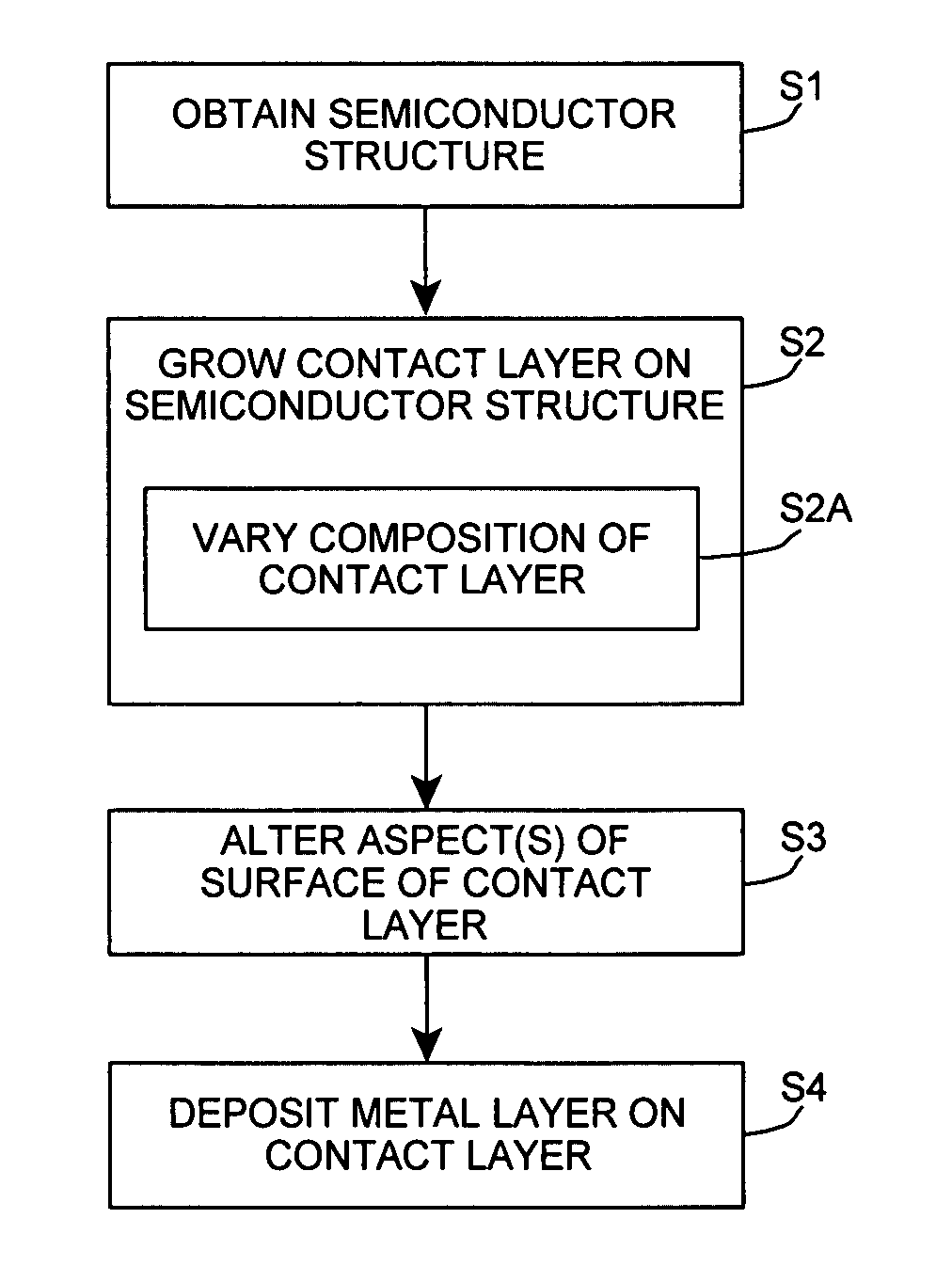
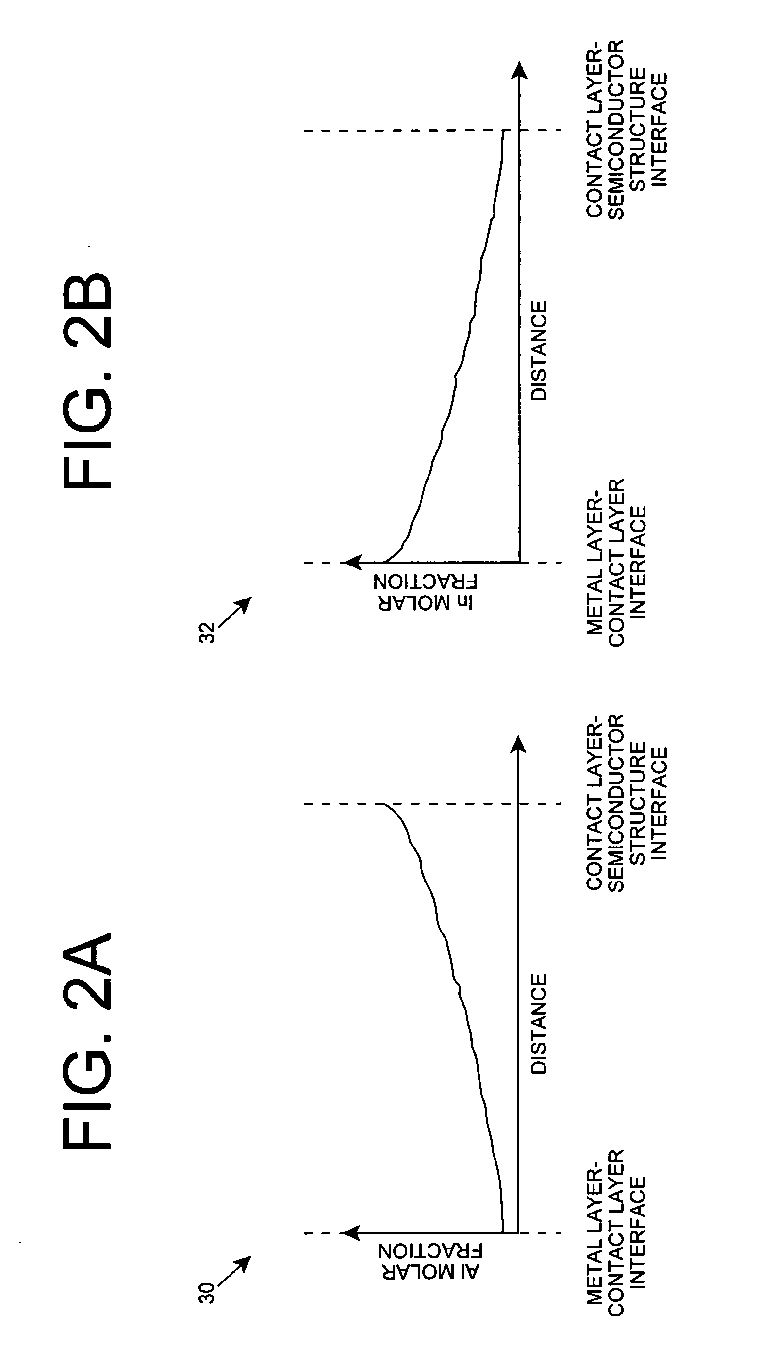
[0024] As indicated above, the invention provides an improved ohmic contact for a nitride-based semiconductor device. In particular, a semiconductor device and method of manufacturing the semiconductor device are provided in which a semiconductor structure has an ohmic contact that includes a contact layer and a metal layer thereon. The contact layer includes at least Aluminum (Al) and Indium (In), and can further include Gallium (Ga) and / or Nitrogen (N). The molar fraction of Al and / or In can be increased / decreased within the contact layer. Additionally, one or more aspects of the surface of the contact layer can be altered prior to depositing the metal layer thereon.

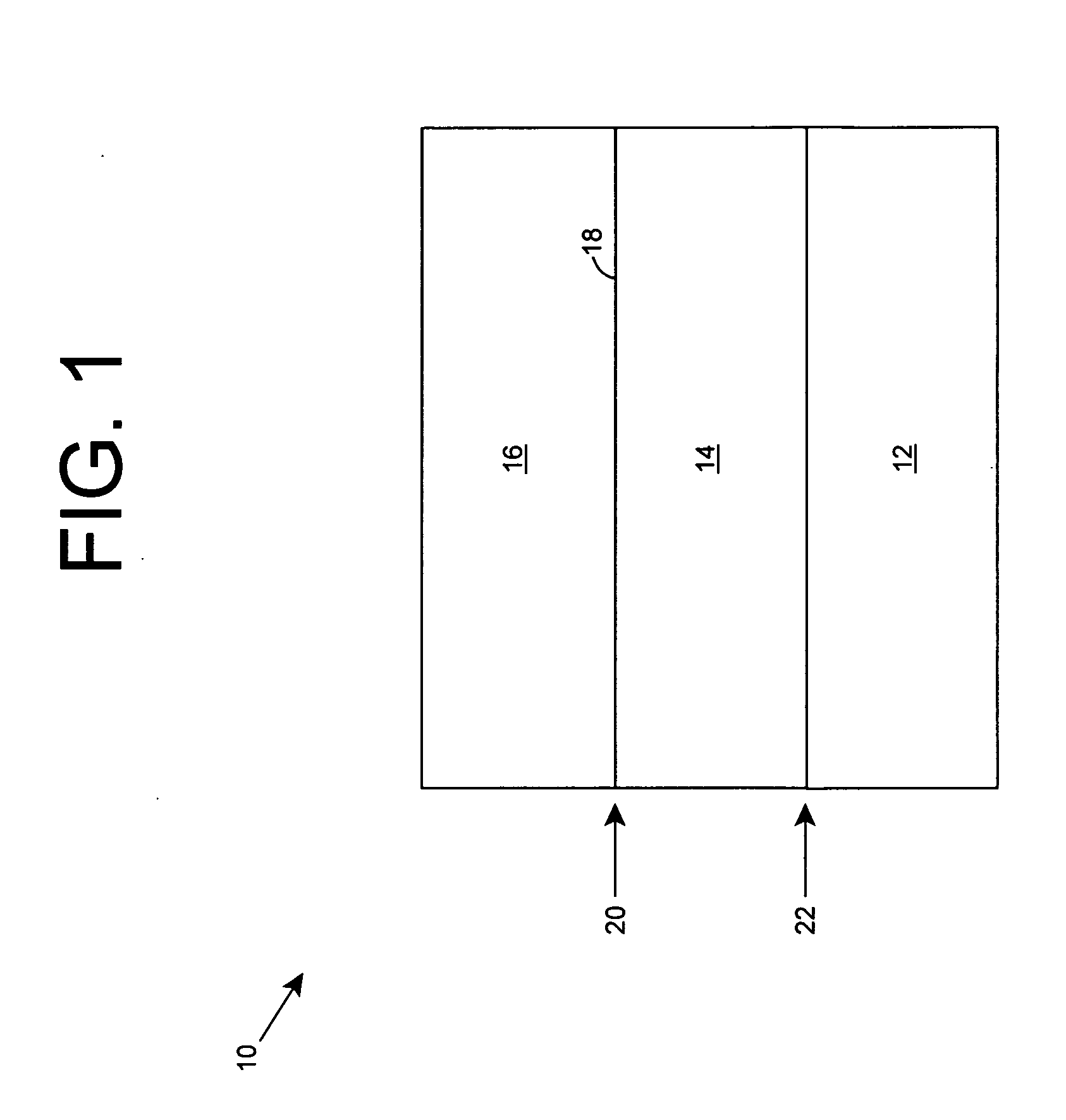
[0025] Turning to the drawings, FIG. 1 shows an illustrative ohmic contact for a nitride-based semiconductor device 10 according to an embodiment of the invention. Device 10 includes a nitride-based semiconductor structure 12, a contact layer 14 on semiconductor structure 12, and a metal layer 16 on contact layer 14. ...


PUM


Abstract

An improved ohmic contact for a nitride-based semiconductor device is provided. In particular, a semiconductor device and method of manufacturing the semiconductor device are provided in which a semiconductor structure has an ohmic contact that includes a contact layer and a metal layer thereon. The contact layer includes at least Aluminum (Al) and Indium (In), and can further include Gallium (Ga) and / or Nitrogen (N). The molar fraction of Al and / or In can be increased / decreased within the contact layer.

Description

REFERENCE TO PRIOR APPLICATION [0001] The current application claims the benefit of co-pending U.S. Provisional Application No. 60 / 604,218, entitled “Ohmic Contact to p-Type Nitride Semiconductor”, which was filed on Aug. 25, 2004, and which is hereby incorporated herein by reference.BACKGROUND OF THE INVENTION [0002] 1. Technical Field [0003] The invention relates generally to ohmic contacts, and more specifically, to an improved ohmic contact for a nitride-based semiconductor device. [0004] 2. Background Art [0005] A challenge in developing high power III-V nitride-based semiconductor devices, such as light emitting diodes, laser diodes, bipolar junction transistors, and heterojunction bipolar transistors, is the development of an ohmic contact that has both a low specific resistance and a high current carrying capability. Magnesium (Mg), with a room-temperature activation energy as high as two hundred fifty meV, is a commonly used acceptor for p-type Gallium Nitride (GaN) semicon...

Claims


Application Information

Patent Timeline
IPC IPC(8): H01L21/3205H01L21/28H01L31/111H01L29/74H01L29/423
CPCH01L21/28575H01L29/452H01L29/2003
Inventor GASKA, REMIGIJUSZHANG, JIANPINGSHUR, MICHAEL
Owner SENSOR ELECTRONICS TECH
Why Eureka
Eureka Blog
Learn More