
Method and apparatus for a sense amplifier

a sense amplifier and random access technology, applied in the field of magnetic random access memories, can solve the problems of data loss, complex control circuitry to continually refresh, leakage,

Active Publication Date: 2006-03-09
SAMSUNG ELECTRONICS CO LTD
View PDF12 Cites 27 Cited by
  • Summary
  • Abstract
  • Description
  • Claims
  • Application Information

AI Technical Summary

Benefits of technology

[0024] One aspect of the present invention is an apparatus, comprising an input node configured to receive an input signal representing a stored value and a gain stage, coupled to the input node, and configured to receive the input signal and to sense if the input signal is less than a reference signal or not less the reference signal and generate an output s

Problems solved by technology

Unfortunately, this technique requires complex control circuitry to continually refresh the stored charges on the capacitors.
If the charges are not refreshed, they leak away and the data they represent are lost.
Continual refreshing of the stored charges results in increased power dissipation even when the memory is not being used, which is problematic for portable computing devices like laptop computers.
Unfortunately, the high speed is obtained at the expense of high density due to the increased amount of chip area required by the latching circuitry to store each bit.
The lower density also leads to higher cost for SRAM.
The extra circuitry used to store each bit also dissipates a large amount of power.
Another shortcoming of DRAM and SRAM is that they are both volatile memory technologies and so lose their stored data when power is removed.
Volatile memory is problematic for portable electronic devices like laptop computers.
However, there are characteristics of flash memory that are problematic for its use as the memory of a personal computer.
Unfortunately, extremely small feature sizes engender a higher sensitivity to manufacturing variation.
Furthermore, extremely thin lines have high resistance that leads to significant resistance variations between lines of different lengths.
These characteristics are problematic to accurately sensing the resistance of an individual memory cell where the absolute resistance change of the cell between the logical 1 state and the logical 0 state is small compared to resistance variation due to the aforementioned manufacturing variation and line length variation.

Method used


Image

  • Method and apparatus for a sense amplifier
  • Method and apparatus for a sense amplifier
  • Method and apparatus for a sense amplifier

Examples


Embodiment Construction

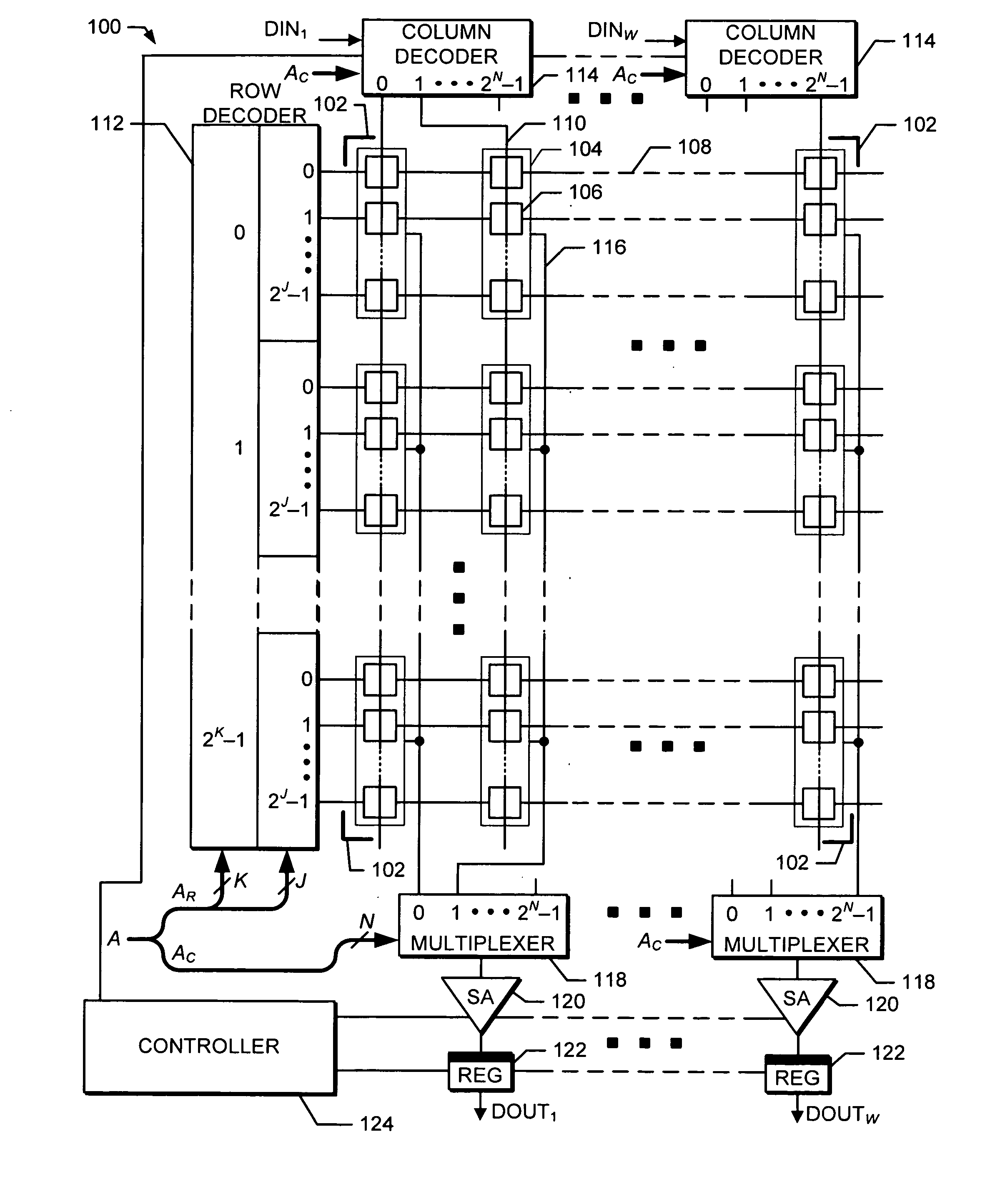
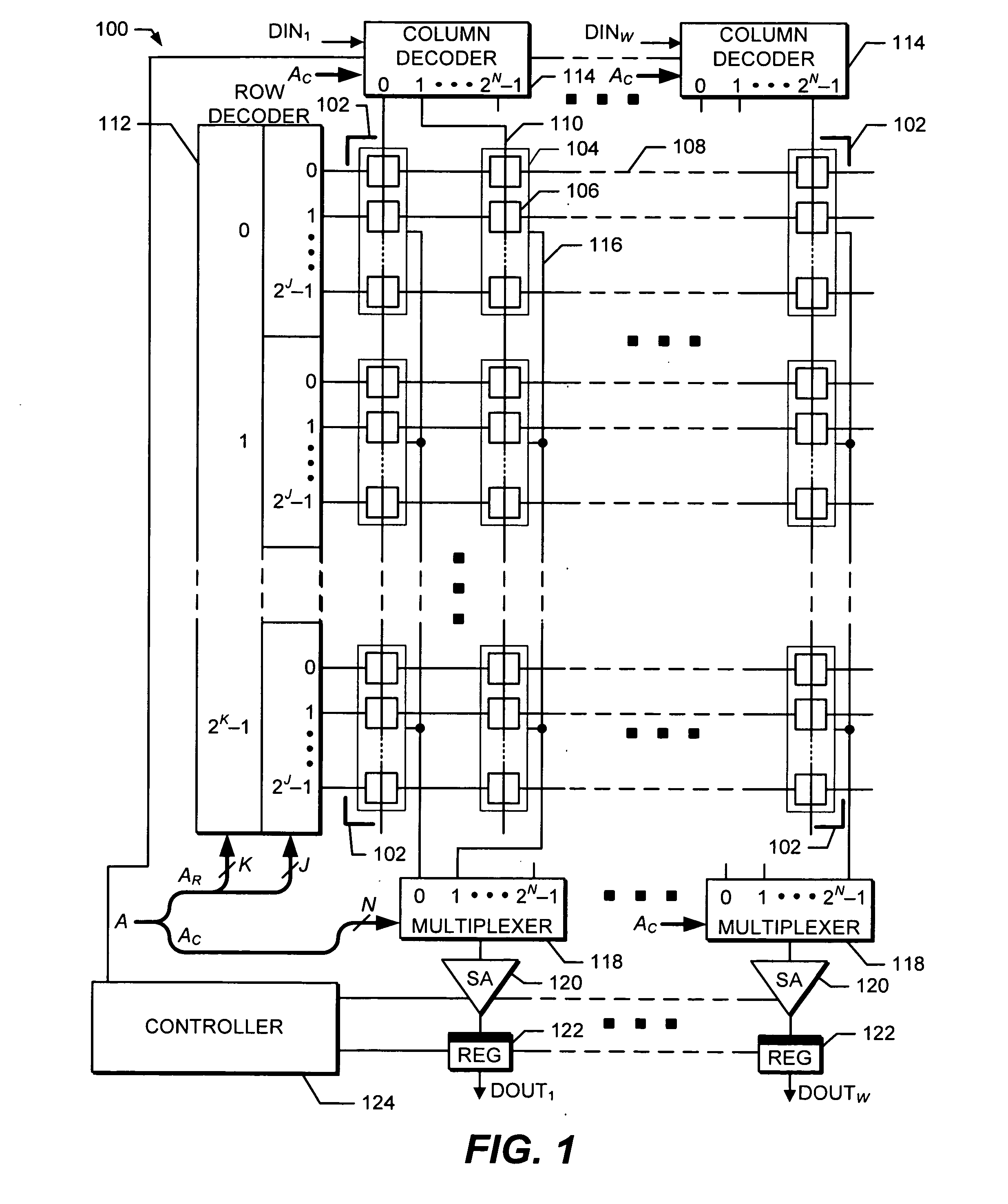
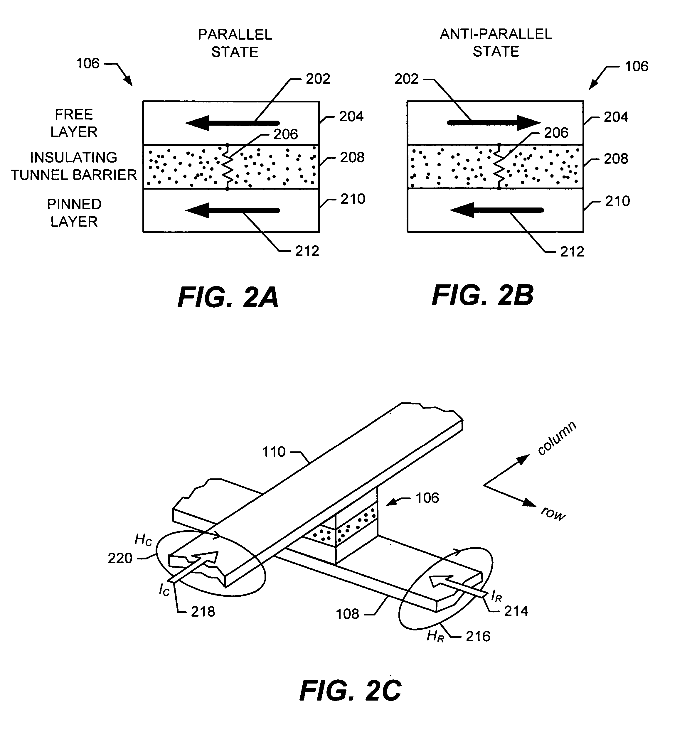
[0028] Implementations of the present invention concern a multi-function circuit to sense and store a first voltage, compare the first voltage with a second sensed voltage, and latch the result of the comparison. Further, the circuit can be placed in a low-power state. The circuit has advantageous application as a sense amplifier for memory technologies such as MRAM where the logical state of a cell is determined by reading the cell's voltage output a first time, writing the cell to a known state, reading the cell's voltage output a second time, and then comparing the two voltages to infer the original state. Hereinafter, the multi-function circuit will be termed simply a “sense amplifier,” even though the circuit also performs the functions of a sample-and-hold circuit, comparator circuit, and latch circuit.

[0029] Implementations of the present invention also concern the use of a single sense amplifier circuit to determine the state of a memory cell in a manner that is relatively ...


PUM


Abstract

A gain stage in a sense amplifier receives an input signal representing a stored value and senses if the input signal is less than or not less than a reference signal and generates an output signal indicative of a first state when the input signal is less than the reference signal and an output signal indicative of a second state when the input signal is not less than the reference signal. The gain stage further comprises an integrated latch configured to latch the output signal in either the first or second state. Additionally, a controller operates a sense amplifier having multiple operating modes. Sample mode switch logic causes the sense amplifier to sample a first voltage applied to the sense amplifier's input and hold and compare mode switch logic causes the sense amplifier to hold the first voltage for comparison with a second voltage applied to the sense amplifier's input.

Description

BACKGROUND [0001] The present invention relates to magnetic random access memories (MRAMs). Electronic appliances such as personal computers use electronic memory for data and program storage. Information is represented as bit patterns in the memory. Each bit can have two states, often referred to as a logical 0 and a logical 1 or just simply as 0 and 1. [0002] Electronic memory often takes the physical form of a small silicon die contained within a plastic or ceramic package for physical protection. The silicon die contains the electronic circuitry of the memory and is a small piece of a larger silicon wafer, which allows a large number of memory “chips” to be manufactured together. Desirable characteristics for computer memory chips are random access, low cost, low power, high density, high speed, and writability. Often one characteristic is obtained at the expense of another. For example, extremely high-speed memory might not be low-cost, high-density, or low-power. Two types of ...

Claims


Application Information

Patent Timeline
IPC IPC(8): G11C7/00
CPCG11C7/062G11C11/16G11C8/10G11C7/065
Inventor PERNER, FREDERICK A.
Owner SAMSUNG ELECTRONICS CO LTD
Learn More