Method for manufacturing vertical cavity surface emitting laser and multiple wavelength surface emitting laser, vertical cavity surface emitting laser, multiple wavelength surface emitting laser, and optical communicating system
- Summary
- Abstract
- Description
- Claims
- Application Information
AI Technical Summary
Benefits of technology
Problems solved by technology
Method used
Image

Examples
first embodiment
(Structure of Multiple Wavelength Surface Emitting Laser)
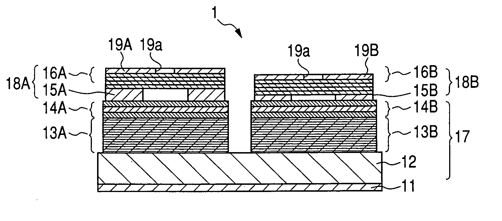
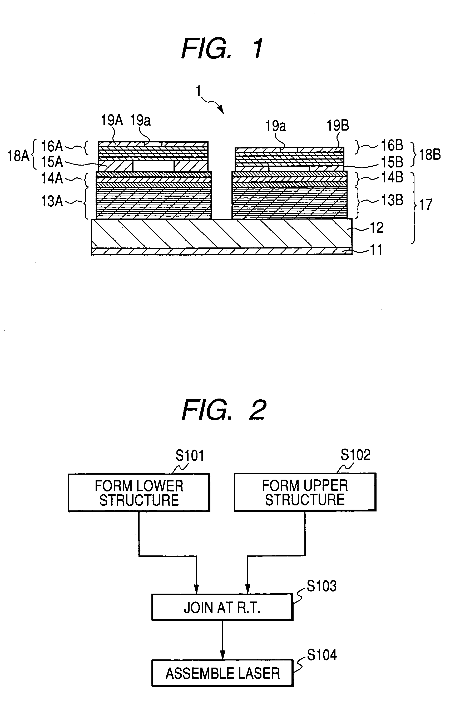
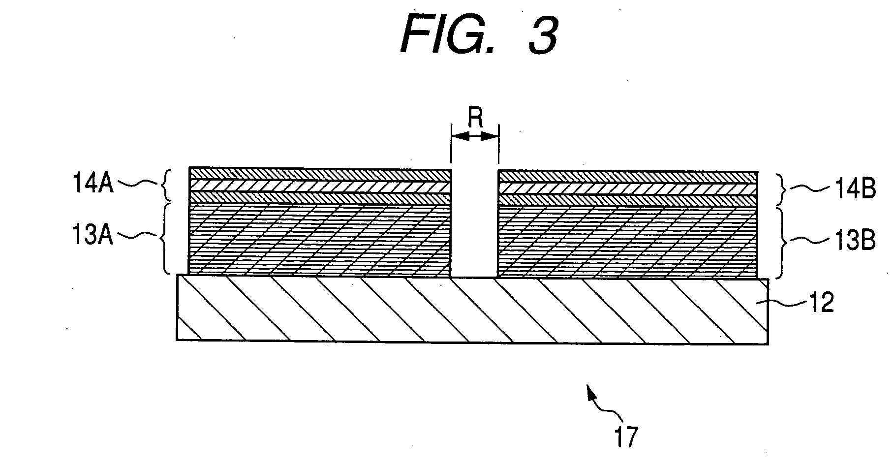
[0033]FIG. 1 shows a structure of a multiple wavelength surface emitting laser according to a first embodiment of the invention. A multiple wavelength surface emitting laser 1 according to this embodiment includes a GaAs substrate 12, two lower DBR layers 13A, 13B, light emitting layers 14A, 14B, annular spacers 15A, 15B, two upper DBR layers 16A, 16B, an n electrode 11, and p electrodes 19A, 19B. The lower DBR layers 13A, 13B serve as a first DBR layer and are formed at a predetermined interval on the GaAs substrate 12. The light emitting layers 14A, 14B of MQW are formed on the respective upper surfaces of the lower DBR layers 13A, 13B. The annular spacers 15A, 15B have different thickness and are formed on the respective upper surface of the light emitting layers 14A, 14B. The upper DBR layers 16A, 16B serve as a second DBR layer and are formed on the respective upper surfaces of the spacers 15A, 15B. The n-electrode 11 i...
second embodiment
[0050]FIG. 7 shows a structure of a multiple wavelength surface emitting laser according to a second embodiment of the invention. The second embodiment is different from the first embodiment in that intermediate DBR layers 50A, SOB are provided on the light emitting layers 14A, 14B, respectively. The other structure and manufacturing steps are the same as those in the first embodiment. The lower structure 17 of this second embodiment includes the GaAs substrate 12, the lower DBR layers 13A, 13B, the light emitting layers 14A, 14B, and the intermediate DBR layers 50A, 50B.
[0051] According to this second embodiment, by joining the upper structures 18A, 18B on the lower structure 17, it is possible to manufacture lasers having different emission wavelengths. Also, since the intermediate DBR layers 50A, 50B are provided in addition to the spacers 15A, 15B, it becomes easy to adjust the wavelengths.
third embodiment
[0052]FIGS. 8A and 8B show manufacturing steps of a multiple wavelength surface emitting laser according to a third embodiment of the invention. The third embodiment is different from the first embodiment in that the spacers 15A, 15B are omitted and that numbers of layers in the upper DBR layers 16A, 16B are made different from each other depending upon the emission wavelengths. The other structure is the same as that in the first embodiment. Incidentally, in FIG. 8, though the upper structures 18A, 18B are shown together, the joining treatment is performed separately.
[0053] First of all, the upper structures 18A, 18B including the upper DBR layers 16A, 16B, which are different in numbers of layers, are prepared separately. Also, the lower structure 17 is prepared in the same manner as that described in the first embodiment.
[0054] Next, as shown in FIG. 8A, the upper DBR layer 16A is precisely positioned in the light outputting position of the light emitting layer 14A. Both joinin...
PUM
 Abstract
Description
Claims
Application Information
 - Generate Ideas
- Intellectual Property
- Life Sciences
- Materials
- Tech Scout
- Unparalleled Data Quality
- Higher Quality Content
- 60% Fewer Hallucinations
Browse by: Latest US Patents, China's latest patents, Technical Efficacy Thesaurus, Application Domain, Technology Topic, Popular Technical Reports.
© 2025 PatSnap. All rights reserved.Legal|Privacy policy|Modern Slavery Act Transparency Statement|Sitemap|About US| Contact US: help@patsnap.com