Method of manufacturing mask for exposure, mask for exposure, and package body of mask for exposure

a technology for masks and packaging, applied in the field of manufacturing masks for exposure, to achieve the effect of good accuracy

Inactive Publication Date: 2006-03-09
FUJITSU MICROELECTRONICS LTD
View PDF9 Cites 3 Cited by
  • Summary
  • Abstract
  • Description
  • Claims
  • Application Information

AI Technical Summary

Benefits of technology

[0009] It is an object of the present invention to provide a method of manufacturing a mask for exposure, a mask for exposure, and a package body of a mask for exposure, where the dimensional fluctuation of a device pattern can be easily guaranteed.
[0011] The above-described measurement of step is not performed generally because it increases the number of processes and there is no need of such measurement. However, a simulation that the inventors of this application performed made it clear that the fluctuation of step affected the dimensional fluctuation of a device pattern. Thus, by obtaining the actual measurement value of step, the dimensional fluctuation of a device pattern can be guaranteed.
[0013] With this configuration, it is possible to determine whether or not the dimensional fluctuation amount of the device pattern falls within the allowable width depending on whether or not the difference between the actual measurement value of the step and the design film thickness of the light-shielding pattern falls into the tolerance, and thus the dimensions of the device pattern can be guaranteed.
[0017] When the contact type step measurement system is used, scanning of the transparent substrate between patterns by the probe of the system is difficult if the distance between adjacent light-shielding patterns is dense. Therefore, in this case, it is preferable that an isolated pattern be provided in a peripheral region of the transparent substrate, the isolated pattern and the transparent substrate near the pattern be scanned by the probe, and the measurement value is used as the above-described actual measurement value. With this method, the step of the isolated pattern can be easily measured even if the light-shielding pattern is formed in high density to deal with the microfabrication of device, so that the dimensional fluctuation of the device pattern can be controlled based on the step.
[0020] Since the actual measurement value written on the above-described inspection result card is obtained by directly measuring the step, the step can be guaranteed with good accuracy comparing to the case where the step is substituted by the design film thickness of a light-shielding film that is formed on the entire surface of a quartz substrate and leads to difficulty of actual measurement of the film thickness.

Problems solved by technology

However, a simulation that the inventors of this application performed made it clear that the fluctuation of step affected the dimensional fluctuation of a device pattern.

Method used


Image

  • Method of manufacturing mask for exposure, mask for exposure, and package body of mask for exposure
  • Method of manufacturing mask for exposure, mask for exposure, and package body of mask for exposure
  • Method of manufacturing mask for exposure, mask for exposure, and package body of mask for exposure

Examples


first embodiment

[0082] (2) First Embodiment

[0083] Next, the manufacturing method of a mask for exposure according to the first embodiment of the present invention will be explained.

[0084]FIG. 7 is the flowchart showing the manufacturing method of a mask for exposure according to this embodiment, and FIG. 8 is the sectional view of the mask for exposure formed by this embodiment. In FIG. 8, reference numerals same as the ones used in FIG. 1D are attached to elements that was already described in FIG. 1D, and their explanation will be omitted. Further, FIG. 9 is the graph of the line width fluctuation amount (CD) of device pattern to the step fluctuation amount, which is used in this embodiment.

[0085] The steps S1 to S8 shown in FIG. 7 are performed not only to a mask for exposure for test but also to all masks for exposure 5.

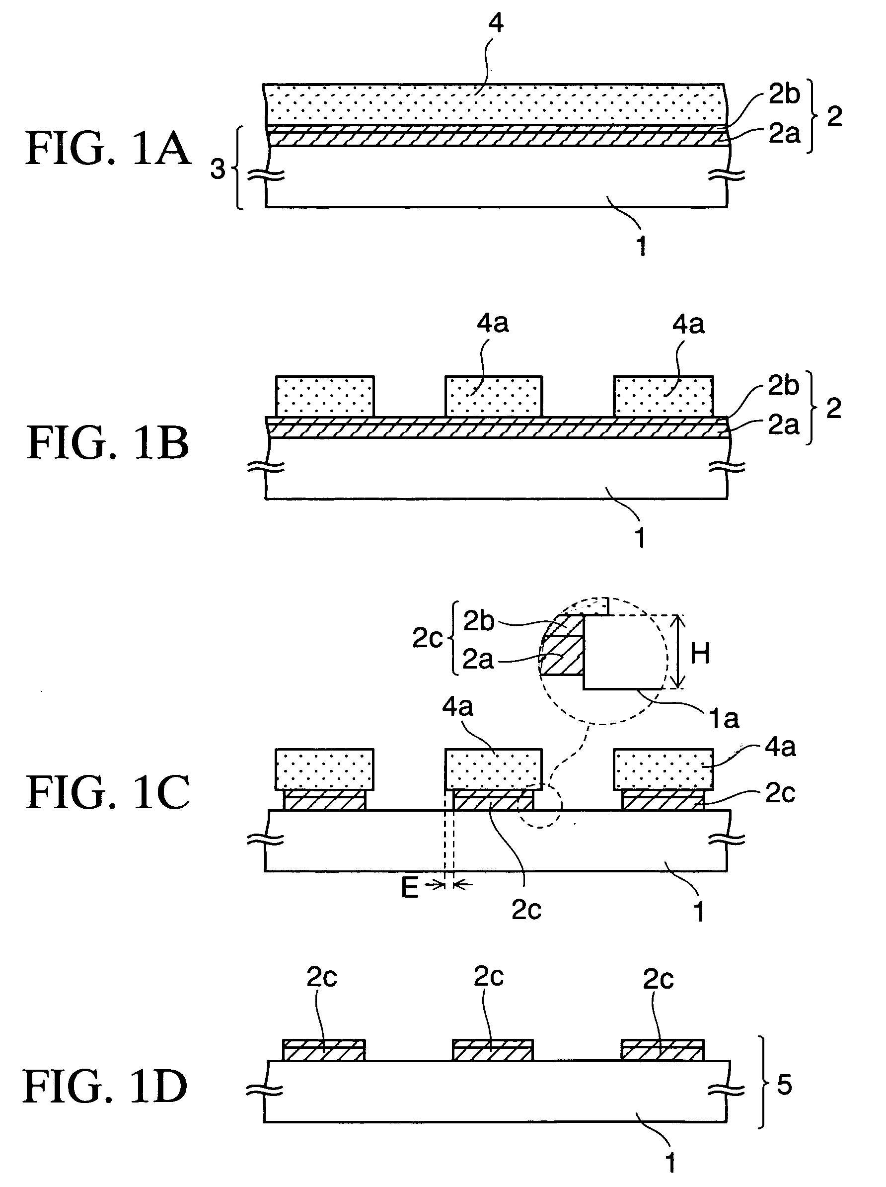
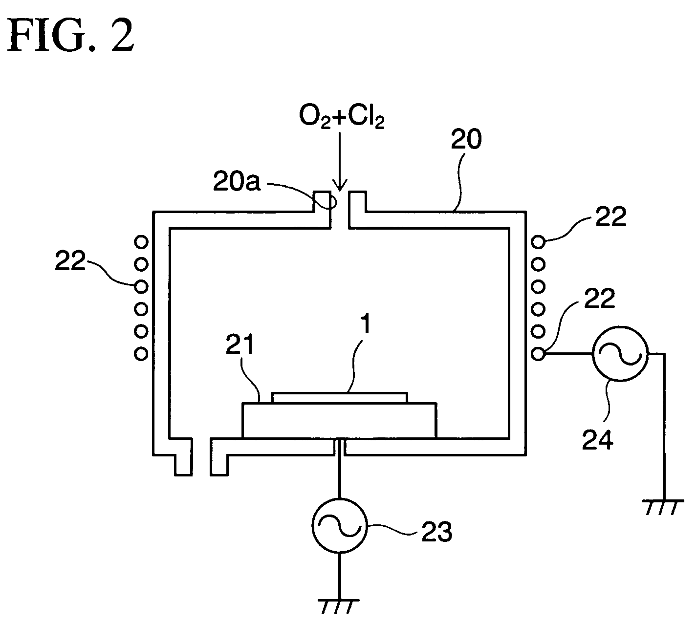
[0086] On step S1, the mask for exposure 5 shown in FIG. 8 is fabricated by following the described FIGS. 1A to 1D. In this embodiment, a substrate having the planar size of ...

second embodiment

[0116] (3) Second Embodiment

[0117] Next, the mask for exposure according to the second embodiment will be explained.

[0118]FIG. 13 is the plan view of the mask for exposure according to this embodiment.

[0119] In the first embodiment, the actual measurement value of the step H was obtained using the AFM system on step S7 of FIG. 7. On the contrary, description in this embodiment will be made for the mask for exposure 5 that is preferable for measuring the step H by the contact type step measurement system.

[0120]FIG. 12 is the sectional view in the case of measuring the step H by the contact type step measurement system.

[0121] In this system, as shown in the drawing, the tip of a probe 40 is allowed to come into contact with the surface of the quartz substrate 1 or the light-shielding pattern 2c, the probe 40 is made to scan in one direction under this condition, and the step on the surface is calculated based on the moved amount of the probe 40 in vertical directions corresponding...

third embodiment

[0129] (4) Third Embodiment

[0130]FIG. 14 is the perspective view of the package body of a mask for exposure according to this embodiment.

[0131] The package body 50 for a mask for exposure is made up of a plastic package box 52 that houses the mask for exposure 5 fabricated in the first and second embodiments, and a lid 54 is placed on the package box 52 in the case of transportation.

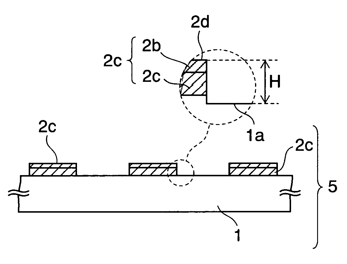
[0132] Further, an inspection result card 53 is attached to the package body 50, on which the actual measurement value of the step H from the surface of the quartz substrate 1 to the top surface of the light-shielding pattern 2c is written, as described in the first and second embodiments. Since the actual measurement value is the one measured on step S4 of FIG. 7 and the value was obtained by directly measuring the step H, the step H can be guaranteed with good accuracy comparing to the case where the step H is substituted by the design film thickness of the light-shielding film 2 guaranteed by the bl...


PUM

PropertyMeasurementUnit
thicknessaaaaaaaaaa
thicknessaaaaaaaaaa
thicknessaaaaaaaaaa

Abstract

There are provided a method of manufacturing a mask for exposure, which includes the step of patterning a light-shielding film formed on a quartz substrate to form a light-shielding pattern, and the step of directly measuring a step from the surface of the quartz substrate to the top surface of the light-shielding pattern to obtain the actual measurement value of the step.

Description

CROSS-REFERENCE TO RELATED APPLICATIONS [0001] This application is based on and claims priority of Japanese Patent Application No. 2004-262511 filed on Sep. 9, 2004, the entire contents of which are incorporated herein by reference. BACKGROUND OF THE INVENTION [0002] 1. Field of the Invention [0003] The present invention relates to a method of manufacturing a mask for exposure, a mask for exposure, and a package body of a mask for exposure. [0004] 2. Description of the Prior Art [0005] In recent years, semiconductor devices have increasingly become further microfabrication, and the minimum dimension of a device pattern has reached as fine as 90 nm. To form such an extremely fine device pattern, it is necessary that not only light having short wavelength (193 nm) of an ArF laser or the like be used as exposure light but also the dimensions of a device pattern, which is obtained from an exposure pattern of a mask for exposure, be rigorously controlled in exposure process. [0006] The m...

Claims


Application Information

Patent Timeline
Patent Type & Authority Applications(United States)
IPC IPC(8): G03C5/00G03F1/00G03F1/54G03F1/68H01L21/027
CPCG03F1/84
Inventor SATO, YUKIHIRO
Owner FUJITSU MICROELECTRONICS LTD
Why Eureka
Try Eureka