Gallium-nitride based light emitting diode light emitting layer structure

a technology of light-emitting diodes and gallium nitride, which is applied in the direction of nanotechnology, electrical equipment, semiconductor devices, etc., to achieve the effects of improving the lighting efficiency of gan-based leds, facilitating the growth of epitaxial layers, and improving quality

Inactive Publication Date: 2006-03-16
EPISTAR CORP
View PDF1 Cites 9 Cited by
  • Summary
  • Abstract
  • Description
  • Claims
  • Application Information

AI Technical Summary

Benefits of technology

[0006] To overcome the foregoing disadvantages, the present invention provides a number of light-emitting layer structures for the GaN-based LEDs that c

Problems solved by technology

This is a dilemma requirin

Method used


Image

  • Gallium-nitride based light emitting diode light emitting layer structure
  • Gallium-nitride based light emitting diode light emitting layer structure
  • Gallium-nitride based light emitting diode light emitting layer structure

Examples


Embodiment Construction

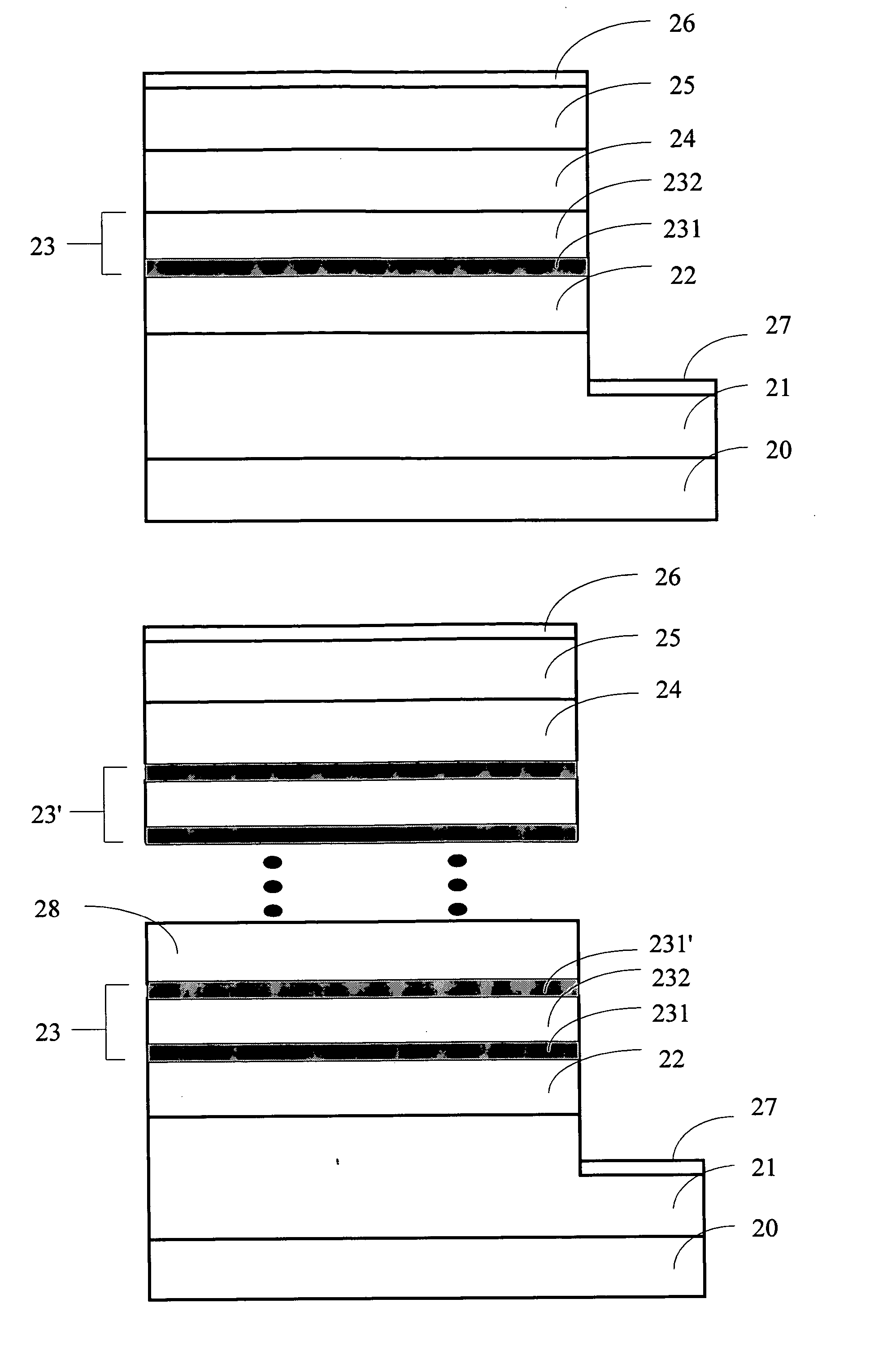
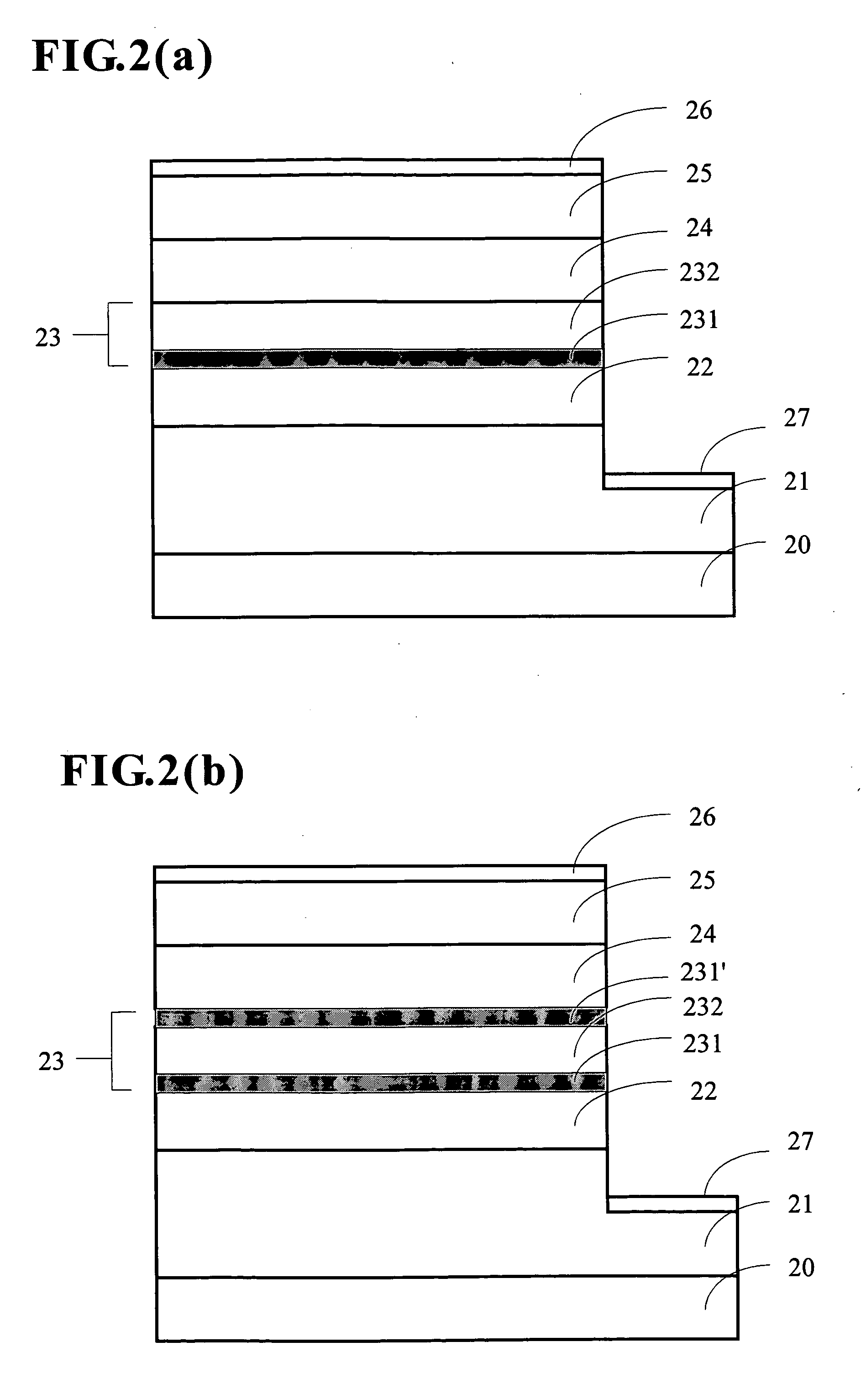
[0015] FIGS. 2(a), 2(b), and 2(c) are schematic diagrams showing the GaN-based LED structures according to a first embodiment of the present invention. As shown in FIGS. 2(a), 2(b), and 2(c), the GaN-based LED structures use sapphire as the substrate 20. Then, sequentially from bottom to top on the sapphire substrate 20, the GaN-based LED structures contain a n-type GaN contact layer 21, a lower barrier layer 22 made of un-doped aluminum-gallium-indium-nitride (Al1-x-yGaxInyN, 0≦x,y≦1, x+y≦1), at least an intermediate layer 23, an upper barrier layer 24 made of un-doped Al1-p-qGapInqN (0≦p,q≦1, p+q≦1), and a p-type GaN contact layer 25. The GaN-based LED structures further contain a positive electrode 26 and a negative electrode 27 on top of the p-type GaN contact layer 25 and the n-type GaN contact layer 21 respectively.

[0016] As shown in FIG. 2(a), the intermediate layer 23 further contains, from bottom to top, an ultra-thin quantum-dot layer 231 made of indium-nitride (InN) and ...


PUM


Abstract

A number of light-emitting layer structures for the GaN-based LEDs that can increase the lighting efficiency of the GaN-based LEDs on one hand and facilitate the growth of epitaxial layer with better quality on the other hand are provided. The light-emitting layer structure provided is located between the n-type GaN contact layer and the p-type GaN contact layer. Sequentially stacked on top of the n-type GaN contact layer in the following order, the light-emitting layer contains a lower barrier layer, at least one intermediate layer, and an upper barrier layer. That is, the light-emitting layer contains at least one intermediate layer interposed between the upper and lower barrier layers. When there are multiple intermediate layers inside the light-emitting layer, there is an intermediate barrier layer interposed between every two immediately adjacent intermediate layers.

Description

BACKGROUND OF THE INVENTION [0001] 1. Field of the Invention [0002] The present invention relates to the gallium-nitride (GaN) based light emitting diode (LED), and in particular to the structure of the light-emitting layer of the GaN-based LED. [0003] 2. The Prior Arts [0004] LEDs have long been widely used as indicators or light sources in various electronic consumer devices due to their features including low power consumption, low heat dissipation, and long operation life. In recent years, researches have been focused on the development of LEDs with various colors and LEDs with high luminance. Among these researches, highly efficient and illuminant blue-light LEDs that can be put to practical use receive the most attention. In October 1995, Nichia Corporation, Japan, announced the successful production of highly illuminant blue-light LEDs based on the indium-gallium-nitride (InGaN) material. This breakthrough has led the world's optoelectronic industry to invest tremendous capit...

Claims


Application Information

Patent Timeline
IPC IPC(8): H01L33/00H01L31/12H01L27/15H01L29/26H01L33/06H01L33/32
CPCB82Y10/00H01L33/32H01L33/06B82Y20/00
Inventor YU, CHENG-TSANGTU, RU-CHINWU, LIANG-WENWEN, TZU-CHICHIEN, FEN-REN
Owner EPISTAR CORP
Why Eureka
Try Eureka