

High electron mobility transistor piezoelectric structures
- Summary
- Abstract
- Description
- Claims
- Application Information
AI Technical Summary
Benefits of technology
Problems solved by technology
Method used
Image

Examples
first embodiment
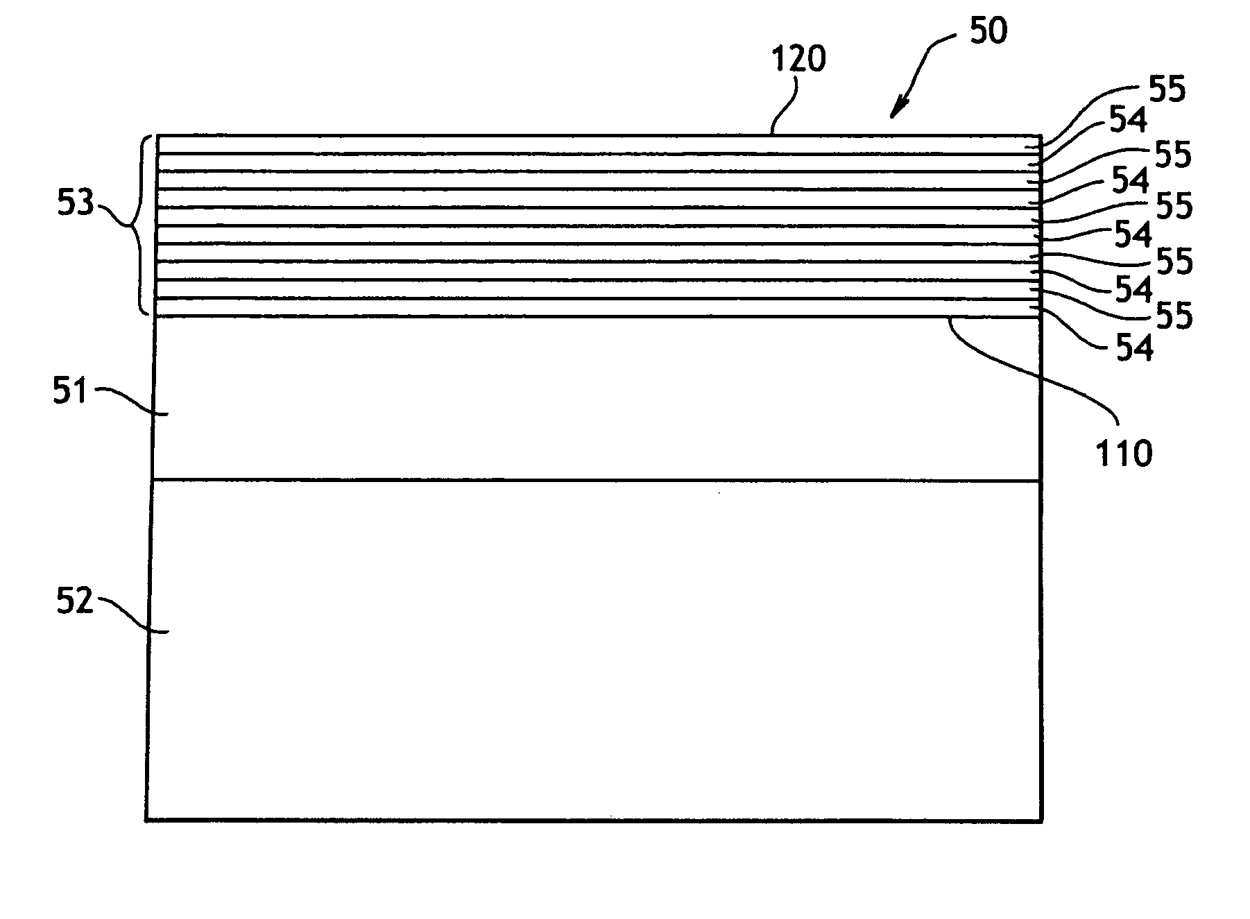
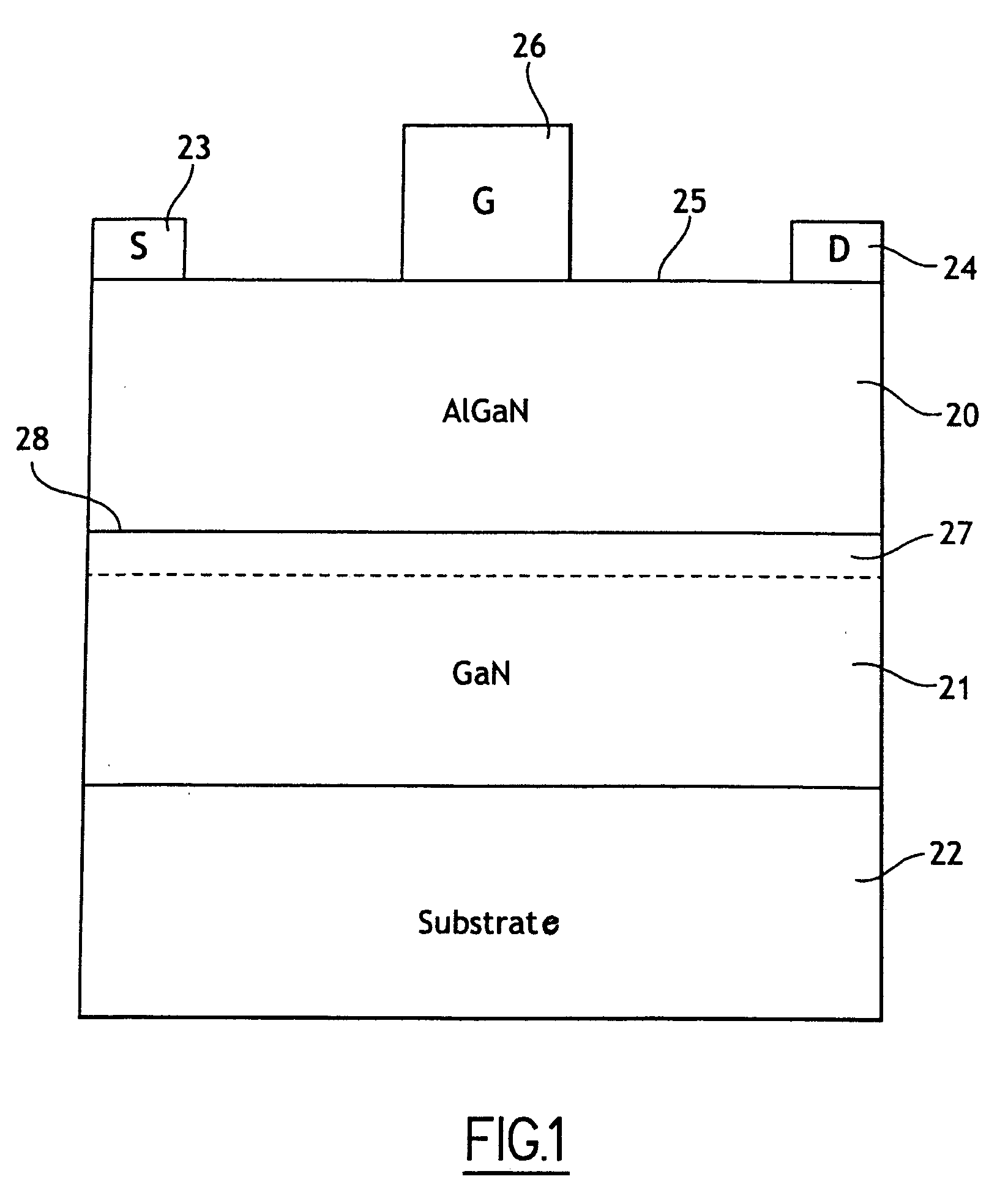
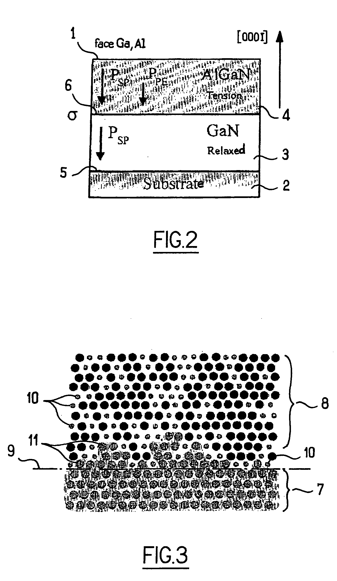
[0074]FIG. 7a illustrates a semiconductor structure 50 according to the invention. This semiconductor structure 50 comprises a channel layer 51 on a support 52, and a barrier layer 53 made of a ternary pseudo-alloy on the channel layer 51.
[0075] The support 52 is made of SiC. However, the support could be made of other materials such as Silicon, AlN, sapphire or GaN. The channel layer 51 is a binary alloy of GaN. However, another material could have been chosen for the channel layer 51, such as AlN, BN (boron nitride) or InN (indium nitride). The channel layer 51 is deposited on the support by a method known to those skilled in the art such as Molecular Beam Epitaxy (MBE) or Metal-Organic Chemical Vapor Deposition (MOVD) method.
[0076] The barrier layer 53 is a ternary pseudo-alloy of AlGaN. The barrier layer 53 comprises binary alloy layers of GaN 54 and binary alloy layers of AlN 55. The GaN and AlN layers are supplied in an alternating fashion. Each binary alloy layer made of GaN...
second embodiment
[0085]FIG. 7b illustrates a semiconductor structure 60 wherein a buffer layer 56 has been inserted between the channel layer 51 and the support 52. The buffer layer 56 is made of a material chosen from among GaN and AlGaN. This buffer layer facilitates growth of the GaN channel layer, and may be provided by bonding or by depositing the layer in another known manner, such as by epitaxial growth.
third embodiment
[0086]FIG. 7c illustrates a semiconductor structure according to a This semiconductor structure includes a support 52, a channel layer 51 and a barrier layer 53. In this embodiment, the barrier layer 53 comprises GaN layers 54′, 54″, 54′″ without the same number of atomic monolayers nGaN. In particular, layers 54′, 54″, 54′″ comprise eight, five and two atomic monolayers of GaN, respectively. These layers alternate with AlN layers 55′ and 55″, the layer 55′ being closest to the support, and the layer 54′″ being furthest from the support. As shown in FIG. 7c, the number of atomic monolayers nGaN per layer of GaN 54′, 54″, 54′″ decreases as the distance from the support 52 increases.
[0087] However, it would be possible to have a barrier layer 53 in which the number of atomic monolayers increases with increasing distance from the support 52. Thus, the number of atomic monolayers nGaN per GaN layer can vary along the barrier layer 53. The same is also true regarding the number of monol...
PUM
 Abstract
Description
Claims
Application Information