Photoelectric conversion device, image pickup device, and method for applying electric field to the same
a technology of photoelectric conversion and image pickup, which is applied in the direction of thermoelectric devices, picture signal generators, radiation control devices, etc., can solve the problems of insufficient luminescent efficiency and device durability, insufficient spectral characteristics, and inability to meet the needs of use, etc., to achieve excellent color reproducibility, high photoelectric conversion efficiency, and excellent durability
- Summary
- Abstract
- Description
- Claims
- Application Information
AI Technical Summary
Benefits of technology
Problems solved by technology
Method used
Image
Examples
example 1
[0161] A cleaned ITO substrate was placed in a vapor deposition apparatus, on which a p-type photoelectric conversion material (Compound 1) was vapor-deposited to 100 nm, and an n-type photoelectric conversion material (Compound 2) was further vapor-deposited to 100 nm, so as to form an organic pn-laminated photoelectric conversion layer. A patterned mask (having a luminescent area of 2 mm×2 mm) was placed on the organic thin film, on which aluminum was vapor-deposited to 500 nm in a vapor deposition apparatus. The assembly was then sealed with a desiccant to produce a photoelectric conversion device for green light (Device No. 101).
example 2
[0162] The same procedures as the Device No. 101 in Example 1 were repeated except that after vapor-depositing the p-type photoelectric conversion material (Compound 1), the n-type photoelectric conversion material (Compound 2) was further vapor-deposited thereon to 80 nm, and further the electron transporting material No. 26 was vapor-deposited to 70 nm. The assembly was sealed with an aluminum electrode in the same manner as in Example 1 to produce a photoelectric conversion device (Device No. 102).
example 3
[0168] Devices were produced in the same manners as in Examples 1 and 2, respectively, except that Quinacridone Compound 1 was used instead of the Compound 1, and the thickness of the n-type Compound 2 was changed to 30 nm (Device Nos. 301 and 302). The devices had a sharp photoelectric conversion spectrum and showed good photoelectric conversion efficiency.
TABLE 2ExternalPhotoelectricquantumconversionElectronefficiencyspectrum λmaxp-typen-typetransporting(applied(half valueDevice No.compoundcompoundmaterialvoltage)width)Device No. 301Compound 3Compound 2none5.3% (12 V)540 nm (95 nm)Device No. 302Compound 3Compound 2No. 266.2% (12 V)543 nm (98 nm)
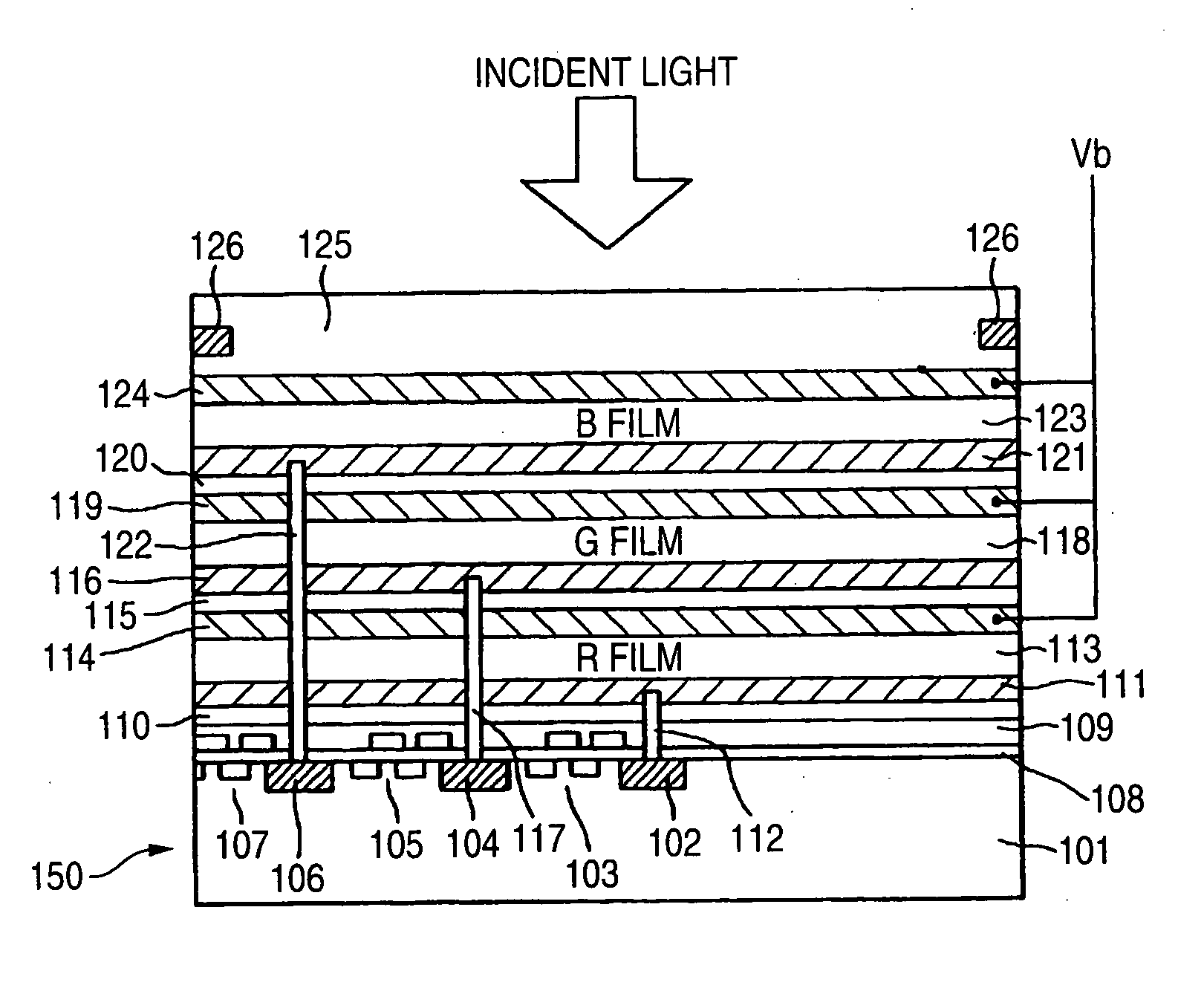
[0169] A three-layer laminated image pickup device shown in FIG. 1 can be produced by combining the aforementioned device with devices for light other than green light, i.e., blue and red light, having the similar design.
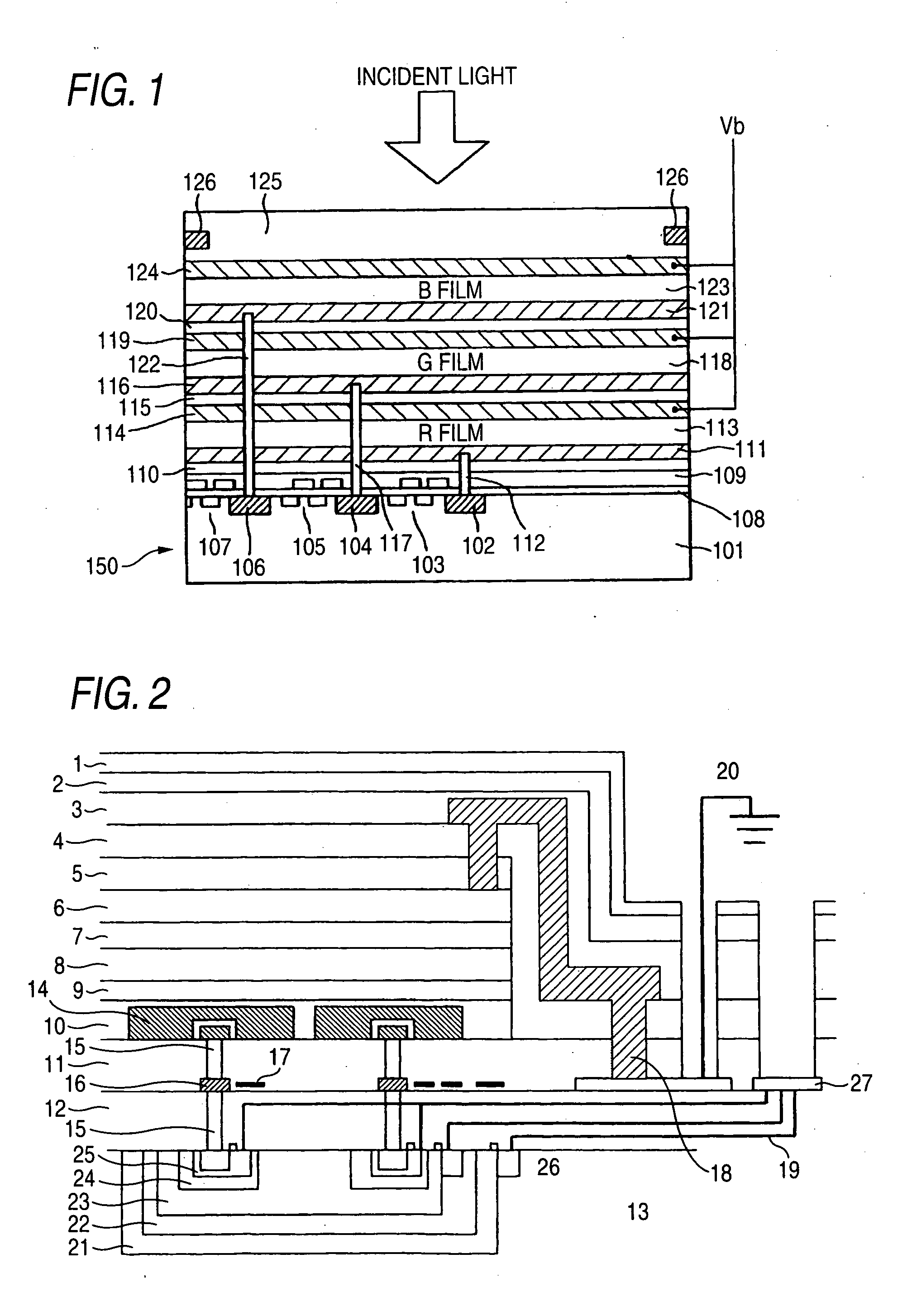
[0170] A device having an organic layer and an inorganic layer as mixture shown in FIG. 2 can be produced by combining...
PUM
 Abstract
Description
Claims
Application Information


