Method of forming a surface mountable IC and its assembly

a technology of integrated circuits and flip-chips, which is applied in the direction of printed circuit aspects, climate sustainability, electrical equipment, etc., can solve the problems of high manufacturing cost of flip-chip assembly of rfid tags, inability to use labels on metal objects, and inability to use isotropic electrical conductivity adhesives (icas), etc., to achieve wide alignment tolerance and increase productivity

Inactive Publication Date: 2006-03-16
AGENCY FOR SCI TECH & RES
View PDF16 Cites 19 Cited by
  • Summary
  • Abstract
  • Description
  • Claims
  • Application Information

AI Technical Summary

Benefits of technology

[0019] These objects are accomplished by designing the RFID chip terminal pads and the corresponding antenna terminal pads on the substrate in a way that the footprint of the connection complies with the footprint of standard discrete SMD. This provides a relatively large interconnect pad area which provides a wide alignment tolerance. The key benefit of designing and fabricating the RFID chip into the form of the standard discrete SMD footprint is that placement of the chip onto the substrate can be carried out with an SMT (Surface Mount Technology) placement machine which is well known in the assembly of printed circuit boards, and is capable of much greater productivity than conventional, critical alignment, flip chip bonding tools.

Problems solved by technology

A disadvantage of this is that the labels cannot be used on metal objects.
Isotropic electrically conducting adhesives (ICAs) are not recommended because they must be applied locally and also require long curing times.
The main disadvantage of the existing RFID tag assembly using the flip-chip process is still high manufacturing cost.
This is driven mainly by low productivity, arising from the slow IC alignment and bonding process which involves the application of heat for an extended period under bonding pressure.
A further problem with the use of ACA is that the interconnect pressure bonding and adhesive curing must be done on the placement machine which creates a serious production bottleneck.
The high manufacturing cost and low productivity is still the main obstacle that prevents widespread adoption of the RFID tag.

Method used


Image

  • Method of forming a surface mountable IC and its assembly
  • Method of forming a surface mountable IC and its assembly
  • Method of forming a surface mountable IC and its assembly

Examples


Embodiment Construction

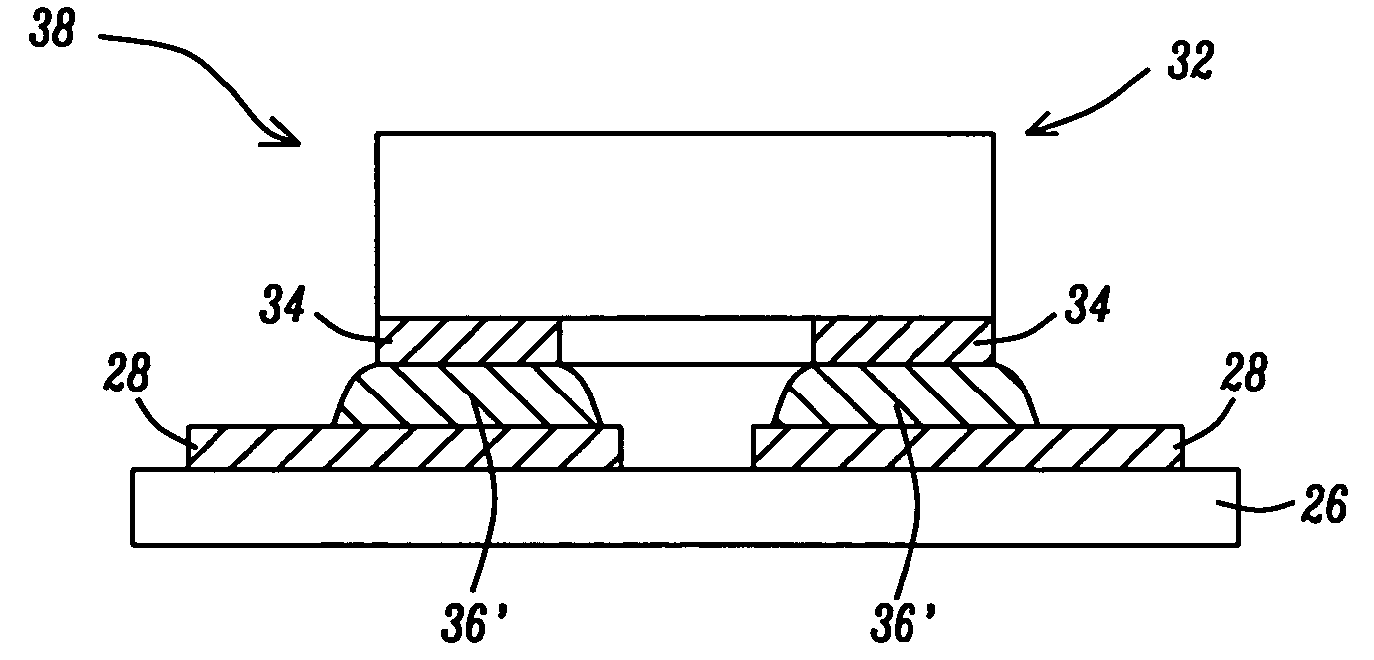
[0024] In a first embodiment of this invention a novel assembly process for mounting an RFID tag on an antenna bearing substrate is described. A key feature of the process is the use of a chip of discrete SMD terminal footprint to mount and interconnect the chip to the substrate, using an isotropic electrically conductive adhesive.

[0025] Referring now to FIGS. 3a, 3b and 3c, a RFID tag integrated circuit chip 32 having a standard discrete SMD terminal footprint is shown. RFID chip 32 is to be mounted and interconnected to an rf antenna 28 which has been patterned on substrate 26. The RF antenna is formed by patterning and curing a conductive paste on the substrate 26. Alternately the RF antenna 28 may be formed by patterning a metal sheet which has been bonded onto the carrier substrate 26. Rf Antenna 28 may be either of coil, dipole, or other two terminal configuration having terminals 30 at locations which, in accordance with standard discrete SMD guidelines are patterned to matc...


PUM


Abstract

A flip-chip interconnect structure for a RFID tag is described which permits the use of an isotropic electrically conductive adhesive (ECA) without requirement of critical alignment of the chip terminal pads to antenna terminals on the substrate. The interconnect foot print utilizes design principles of standard discrete SMD terminal footprint, which does not require alignment accuracy of a NCA/ACA flip chip bonder. The use of an ECA also eliminates the need for curing the adhesive while under heat and pressure on the chip placement machine. Because of the wide placement tolerance the chips can be placed with a low cost highly productive SMT placement machine. After placement, the assemblies leave the placement machine and are cured in an oven, thereby further improving the productivity of the placement machine. Further productivity improvement is realized by the elimination of bumping which is no longer required. The overall cost reduction of the final assembly by the process of the invention is estimated at about 60 to 85 percent.

Description

BACKGROUND OF THE INVENTION [0001] (1) Field of the Invention [0002] The invention relates to processes for the manufacture of integrated circuits and more particularly to the mounting of an integrated circuit chip onto a substrate by a surface mount method [0003] (2) Background of the Invention and Description of Previous Art [0004] Flip chip microelectronic assembly is the direct electrical connection of face-down electronic components or integrated circuit chips onto substrates, circuit boards, or carriers by means of conductive bumps on the chip bond pads. In contrast, wire bonding, the older technology which flip chip replaces, uses face-up chips with a wire connection to each pad. Flip chip components are predominantly semiconductor devices; however, components such as passive filters, detector arrays, and MEMs devices are also beginning to be used in flip chip form. Flip chip is also called Direct Chip Attach (DCA), a more descriptive term, since the chip is directly attached...

Claims


Application Information

Patent Timeline
Patent Type & Authority Applications(United States)
IPC IPC(8): H01L21/44
CPCH01L24/83H01L2224/16225H01L2924/1461H01L2924/07811H01L2924/01006H01L2224/73204H01L2224/83192H01L2224/838H01L2924/01005H01L2924/01013H01L2924/01027H01L2924/01046H01L2924/01047H01L2924/01074H01L2924/01079H01L2924/01082H01L2924/0781H01L2924/14H05K3/321H05K2201/10636H01L24/29H01L2924/00H01L2224/0554H01L2224/05568H01L2224/05573H01L2924/00014Y02P70/50H01L2224/05599H01L2224/0555H01L2224/0556
Inventor TEO, POI SIONGCHONG, SER CHOONGSRINIVASAMURTHY, SAMPATH
Owner AGENCY FOR SCI TECH & RES
Why Eureka
Try Eureka