Production methods for a leadframe and electronic devices

a technology of electronic devices and leadframes, applied in semiconductor devices, semiconductor/solid-state device details, electrical apparatus, etc., can solve problems such as unusability of electronic devices

Inactive Publication Date: 2006-03-23
INFINEON TECH AG
View PDF7 Cites 22 Cited by
  • Summary
  • Abstract
  • Description
  • Claims
  • Application Information

AI Technical Summary

Benefits of technology

[0029] In accordance with a further mode of the invention, the application of a conductive material is by currentless electrodeposition. A currentless electrodeposition has the advantage that an electrical voltage does not have to be applied to the leadframe. Rather, the leadframe is immersed in the deposition bath and withdrawn with a currentlessly deposited metal layer. During the stripping of the patterned insulating layer, the desired rivet-shaped cross-sections form in envisaged surface regions for the external contact elements.
[0030] At the same time as the external contact elements a metallic base may be formed in the chip carrier region of the lead frame. Such a metallic base has the advantage that, by way of example, the underside of the semiconductor chip can be contact-connected therewith. In principle, any desired geometrical structure that serves for the formation of external contact area configurations can be deposited on the basic substrate by the method according to the invention.

Problems solved by technology

In such a case, there is the risk that, during the production or during the operation of the electronic device, the external contact elements will become detached from the plastics compound and the electronic device will, thus, become unusable.

Method used


Image

  • Production methods for a leadframe and electronic devices
  • Production methods for a leadframe and electronic devices
  • Production methods for a leadframe and electronic devices

Examples


first embodiment

[0073] If the basic substrate 11 is a metallic foil as in the exemplary embodiment of FIG. 6, then the metallic foil can be removed by wet or dry etching after the injection-molding of the plastic before or during the singulation of the electronic devices of a leadframe of the Here, too, it is advantageous if the external contact element 6 has an etching stop layer in the rivet foot region 10.

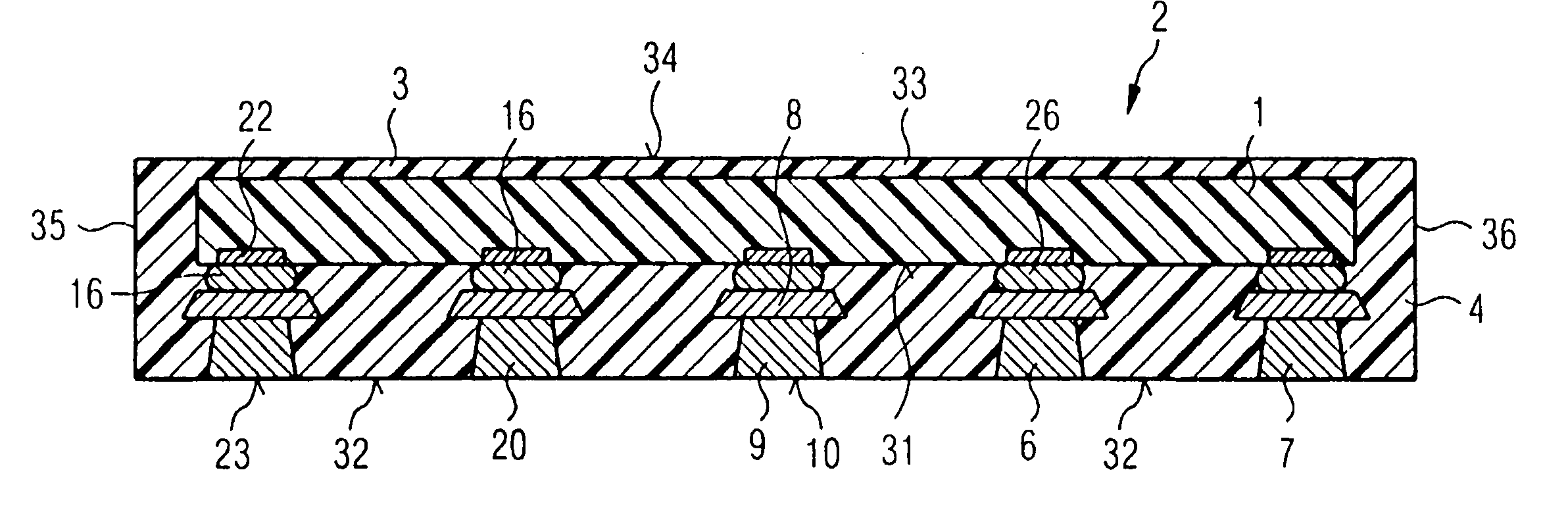
[0074]FIG. 7 shows a diagrammatic cross-section through an electronic device 2 in accordance with a first embodiment of the invention. The electronic device 2 is provided with a housing 3 that is made of plastics compound 4 and is potted on one side, and has a semiconductor chip 1 in the housing 3, which semiconductor chip 1 has contact areas 22 connected to external contact elements 6 through bonding bumps 16 made of soldering balls, for example. The external contact elements 6 have a rivet-shaped cross-section with a rivet foot region 10, a rivet shank region 9, and a rivet head region 8, th...

second embodiment

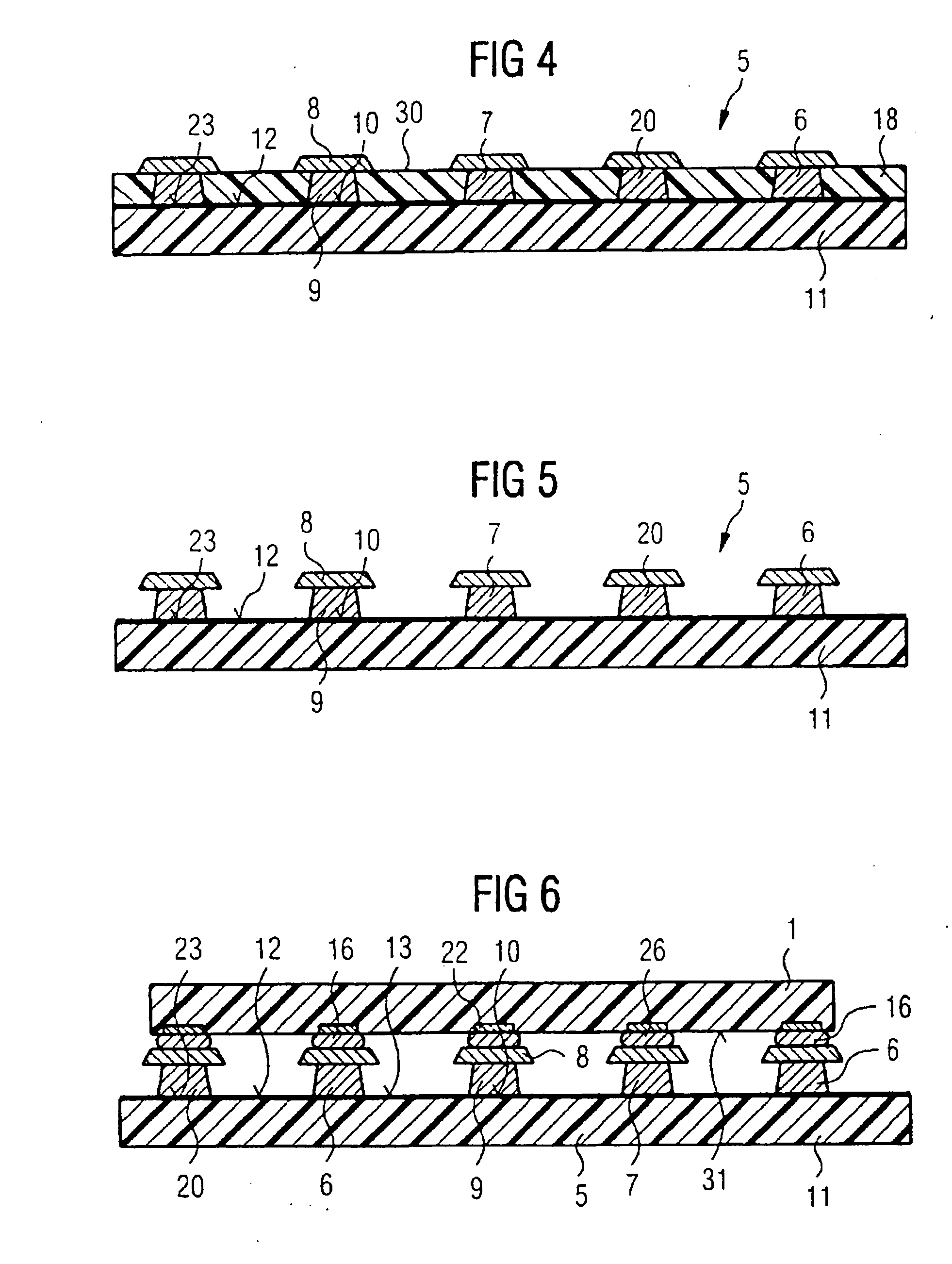
[0077]FIG. 8 shows a diagrammatic cross-section through a leadframe 5 with an applied semiconductor chip 1 in accordance with the invention. The leadframe 5 differs from the leadframe 5 of FIG. 5 in that a metallic base 17 is applied to the basic substrate 11 in the chip carrier region at the same time as the formation of external contact elements 6. In the embodiment of FIG. 8, the metallic base 17 is made of the same material as the external contact elements 6 and has the same height h. The areal extent of the metallic base 17 is adapted to the size of the semiconductor chip 1 so that the semiconductor chip 1 can be applied completely on the metallic base 17, as shown in FIG. 8. The application can be effected by adhesive bonding using a conductive adhesive or by alloying the semiconductor chip 1 onto the metallic base 17.

[0078] In the second embodiment of the leadframe 5, the semiconductor chips 1 are applied to the metallic base 17 with their passive side 33, which does not carr...

third embodiment

[0081]FIG. 11 shows a diagrammatic cross-section through an electronic device in accordance with the invention. This device is distinguished by its extreme planarity because even the base height h, as is shown in FIG. 8, is additionally obviated. A disadvantage of such a device is that the passive side 33 of the semiconductor chip 1 simultaneously forms the underside 32 of the electronic device. The semiconductor chip 1 is, thus, exposed to ambient influences with its underside 33. The external contact elements 6 are securely anchored in the plastics compound 4 of the housing 3 on account of their rivet-shaped cross-section and have, in their rivet foot region 10, a circular plan that provides a circular contact pad as external contact area 23.


PUM


Abstract

A leadframe for semiconductor chips and electronic devices produced on the leadframe includes providing the leadframe with a basic substrate, on which are disposed external contact elements exhibiting a rivet-shaped cross-section with a rivet head region, a rivet shank region, and a rivet foot region, as a result of which, the external contact elements are securely anchored in the housing made of a plastics compound.

Description

CROSS-REFERENCE TO RELATED APPLICATIONS [0001] This is a divisional application of application Ser. No. 10 / 330,440, filed Dec. 27, 2002; which was a continuing application, under 35 U.S.C. §120, of International application PCT / DE01 / 02097, filed Jun. 7, 2001; the application also claims the priority, under 35 U.S.C. §119, of German patent application DE 100 31 204.7, filed Jun. 27, 2000; the prior applications are herewith incorporated by reference in their entirety.FIELD OF THE INVENTION [0002] The invention relates to production methods for a leadframe and electronic devices. [0003] Leadframes for semiconductor chips for packing the semiconductor chips to form electronic devices in housings made of a plastics compound have to satisfy high reliability despite their mass production. This is true particularly if the leadframe is to be used to produce housings from which no flat conductors whatsoever protrude as terminal pins or terminal legs and, in the case of which, the housing mad...

Claims


Application Information

Patent Timeline
Patent Type & Authority Applications(United States)
IPC IPC(8): H01L23/48H01L23/12H01L21/56H01L21/68H01L23/31H01L23/485
CPCH01L21/56H01L21/568H01L23/3107H01L24/48H01L2224/11003H01L2924/01068H01L2224/16H01L2224/48471H01L2924/01079H01L2924/19043H01L2224/1147H01L2224/05599H01L2224/45099H01L2224/85399H01L2924/00014H01L2924/12042H01L2924/181H01L2924/00H01L2224/45015H01L2924/207H01L2924/00012H01L21/60
Inventor PAULUS, STEFAN
Owner INFINEON TECH AG
Why Eureka
Try Eureka