High-speed differential logic buffer

Active Publication Date: 2006-03-23
ANALOG DEVICES INC
View PDF2 Cites 18 Cited by
  • Summary
  • Abstract
  • Description
  • Claims
  • Application Information

AI Technical Summary

Benefits of technology

[0007] Embodiments of the present invention are directed to an active load circuit connected to an output of a high speed digital buffer, and to methods of operating such a circuit. The active load circuit loads the buffer output with an active inductance stage h

Problems solved by technology

However, CML circuits draw relatively high power and may have limited speed in a given process technology.
But in integr

Method used


Image

  • High-speed differential logic buffer
  • High-speed differential logic buffer
  • High-speed differential logic buffer

Examples


Embodiment Construction

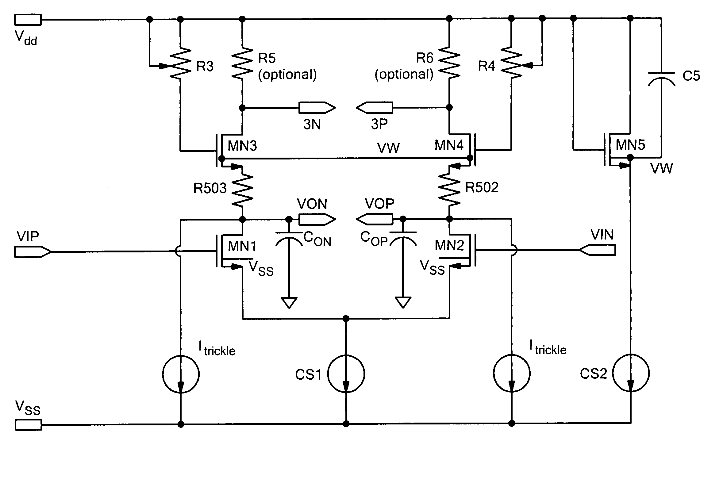
[0023] Various embodiments of the present invention are directed to techniques for using an active inductance stage load circuit to reduce the rise and fall times at the output terminals of a high speed digital buffer. This allows for significant improvement in stage bandwidth, which can be used to run circuits faster at a given current level or to maintain speed at a lower current level (thereby reducing power consumption). This facilitates implementation of high-speed digital circuits such as crosspoint switches. Embodiments of the present invention allow approximately a doubling of speed at a given power, or halving of power at a given speed, with low area penalty. Because some embodiments can be implemented with only resistors and transistors, they are better suited for implementation in integrated circuits than the older passive inductor approach.

[0024]FIG. 4 shows the circuit structure for an active load buffer according to one embodiment of the present invention. One specifi...


PUM


Abstract

A circuit for a high speed digital buffer has an active load circuit connected to an output of the digital buffer. The active load circuit loads the buffer output with an active inductance to reduce the RC time constant at the buffer output. The active load circuit may be based on two active devices connected to the buffer output so as to form a differential cascode circuit.

Description

FIELD OF THE INVENTION [0001] The invention generally relates to data switching circuits, and more specifically to an active load circuit for a high speed logic buffer. BACKGROUND ART [0002] Current mode logic (CML) circuits are often used to implement high speed serial digital communications applications. Such circuits typically use resistively-loaded differential switch arrangements which can provide high speed, low supply noise generation, and high supply noise immunity. However, CML circuits draw relatively high power and may have limited speed in a given process technology. [0003] One specific example of a high speed digital circuit is a crosspoint switch, which can selectably connect data signals between multiple inputs and multiple outputs. FIG. 1 shows the functional block architecture of a typical crosspoint switch. The left edge of the figure shows inputs 0-39 and the bottom edge shows outputs 0-35. Any input can be connected to any number of outputs. Each of the smaller d...

Claims


Application Information

Patent Timeline
IPC IPC(8): H03K19/094
CPCH03K19/09432H03K19/01707
Inventor TAM, KIMO Y. F.
Owner ANALOG DEVICES INC
Why Eureka
Try Eureka