Image display device

Inactive Publication Date: 2006-03-30
HITACHI LTD
View PDF3 Cites 18 Cited by
  • Summary
  • Abstract
  • Description
  • Claims
  • Application Information

AI Technical Summary

Benefits of technology

[0052] According to the present invention, the taper angle of the edge of the interlayer insulator can be made small enough to prevent disconnection in the upper electrode formed between the cathode and the upper bus electrode. In addition, due to the small taper angle of the interlayer insulator, it is easy to thicken the interlayer insulator. Accordingly, it is possible to reduce the capacitance of the crossing portion where a scan signal electrode crosses the data line, that is, a scan signal electrode crosses the

Problems solved by technology

This scan line current leads to a voltage drop along the scan lines due to wiring resistance, so as to prevent uniform operation of the cathodes.
Particularly in order to attain a large-size display device, the voltage drop caused by the wiring resistance of the scan lines becomes a large problem.
However, when the thickness of the base electrode is increased to reduce the resistance, the irregularities of the wiring may be intense, the quality of an e

Method used


Image

  • Image display device
  • Image display device
  • Image display device

Examples


embodiment 1

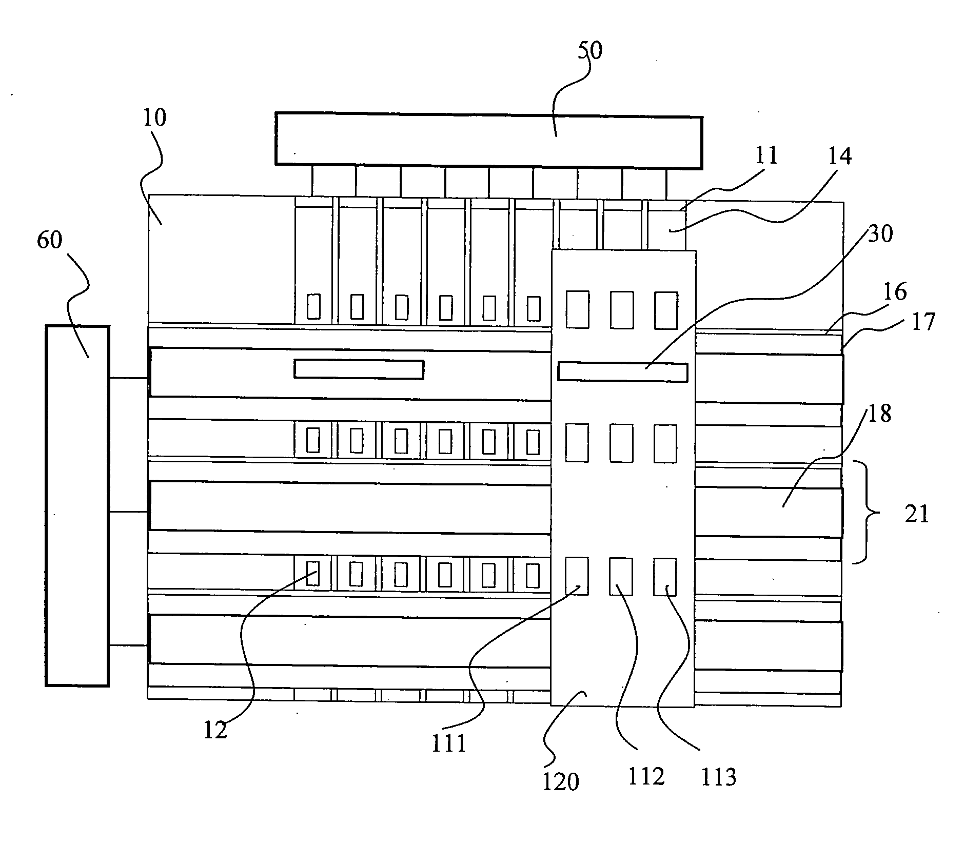
[0085]FIG. 12 is a main portion sectional view for explaining the configuration of Embodiment 1 of an interlayer insulator according to the present invention. In FIG. 12, the field insulator 14 is formed on the base electrode 11 shown in FIG. 11, and the base electrode 11 is formed on the cathode substrate 10 made of a glass plate. However, the base electrode 11 and the cathode substrate 10 are not shown in FIG. 12.

[0086] In Embodiment 1, the interlayer insulator 15 is constituted by a laminated film of a lower layer 15-1 and an upper layer 15-2. The lower layer 15-1 is made of a silicon oxide film SiO2, and formed on the field insulator 14, and a silicon nitride film SiN is formed thereon as the upper layer 15-2. A photo-resist 26 is applied onto the laminated film. The photo-resist 26 is applied to expose a region so as to be formed as a taper.

[0087] The silicon oxide film SiO2 and the silicon nitride film SiN have different dry etching rates. The dry etching rate of the silicon...

embodiment 2

[0090]FIG. 13 is a main portion sectional view for explaining the configuration of Embodiment 2 of an interlayer insulator according to the present invention. Also in FIG. 13, in the same manner as in FIG. 12, the field insulator 14 is formed on the base electrode 11 shown in FIG. 11, and the base electrode 11 is formed on the cathode substrate 10 made of a glass plate. However, the base electrode 11 and the cathode substrate 10 are not shown in FIG. 13.

[0091] In Embodiment 2, the interlayer insulator 15 is constituted by a laminated film of a lower layer 15-3 and an upper layer 15-2. The lower layer 15-3 is made of a silicon oxynitride film SiO2 (x) N (y), and formed on the field insulator 14. Here, (x) designates the content of silicon oxide SiO2, and (y) designates the content of silicon nitride SiN. A silicon nitride film SiN is formed as the upper layer 15-2 on the silicon oxynitride film SiO2(x)N(y).

[0092] The silicon oxynitride film SiO2(x)N(y) 15-3 is a film with a composi...

embodiment 3

[0096]FIG. 14 is a main portion sectional view for explaining the configuration of Embodiment 3 of an interlayer insulator according to the present invention. Also in FIG. 14, the field insulator 14 is formed on the base electrode 11 shown in FIG. 11, and the base electrode 11 is formed on the cathode substrate 10 made of a glass plate. However, the base electrode 11 and the cathode substrate 10 are not shown in FIG. 14.

[0097] In Embodiment 3, as the interlayer insulator 15, only a silicon oxynitride film SiO2 (x)N(y) 15-4 having a composition gradient similar to that of the lower layer in Embodiment 2 is formed on the field insulator 14. Here, (x) designates the content of silicon oxide SiO2, and (y) designates the content of silicon nitride SiN.

[0098] In the silicon oxynitride film SiO2(x)N(y) 15-4, the value (x) is remarkably larger than the value (y) on the field insulator 14 side, that is, the silicon oxynitride film SiO2(x)N(y) 15-4 is rich in silicon oxide SiO2 on the field...


PUM


Abstract

An interlayer insulator with a low taper angle is formed as a laminated film in which a silicon nitride film is formed on a silicon oxide film formed on the glass substrate side (field insulator side). Thus, an upper electrode of a cathode formed on the interlayer insulator is prevented from being broken, while a crossing portion between the upper electrode and a base electrode of the cathode is made low in capacitance. At the same time, sodium separated from glass of the substrate is blocked. Disconnection of the upper electrode is prevented due to the low taper angle of the interlayer insulator. Low capacitance is attained by increasing the film thickness of the interlayer insulator. The cathode is prevented from being contaminated with sodium separated from glass of the substrate.

Description

CLAIM OF PRIORITY [0001] The present application claims priority from Japanese application JP 2004-288489 filed on Sep. 30, 2004, the content of which is hereby incorporated by reference into this application. FIELD OF THE INVENTION [0002] The present invention relates to an image display device, and particularly relates to an image display device also referred to as an emissive flat panel display using thin-film electron emitter arrays. DESCRIPTION OF THE BACKGROUND ART [0003] An image display device (Field Emission Display: FED) using field emission cathodes that are microscopic and can be integrated has been developed. The field emission cathodes are also referred to as thin-film cathodes. Cathodes of such an image display device are categorized into field emission cathodes and hot electron emission cathodes. The former includes Spindt type cathodes, surface-conduction electron emission cathodes, carbon-nanotube cathodes, and the like. The latter includes thin-film cathodes of an...

Claims


Application Information

Patent Timeline
IPC IPC(8): H01L29/76
CPCH01J29/481H01J9/027
Inventor KUSUNOKI, TOSHIAKISAGAWA, MASAKAZUTSUJI, KAZUTAKA
Owner HITACHI LTD
Why Eureka
Try Eureka