

Display device and manufacturing method thereof
a technology of a display device and a manufacturing method, which is applied in the direction of identification means, instruments, electroluminescent light sources, etc., can solve the problems of insufficient control of seepage of sealing materials by the scribe line, and achieve the effect of preventing expansion of the width of the seal pattern, and suppressing the reduction of bond strength
- Summary
- Abstract
- Description
- Claims
- Application Information
AI Technical Summary
Benefits of technology
Problems solved by technology
Method used
Image

Examples
embodiment
Embodiment 1
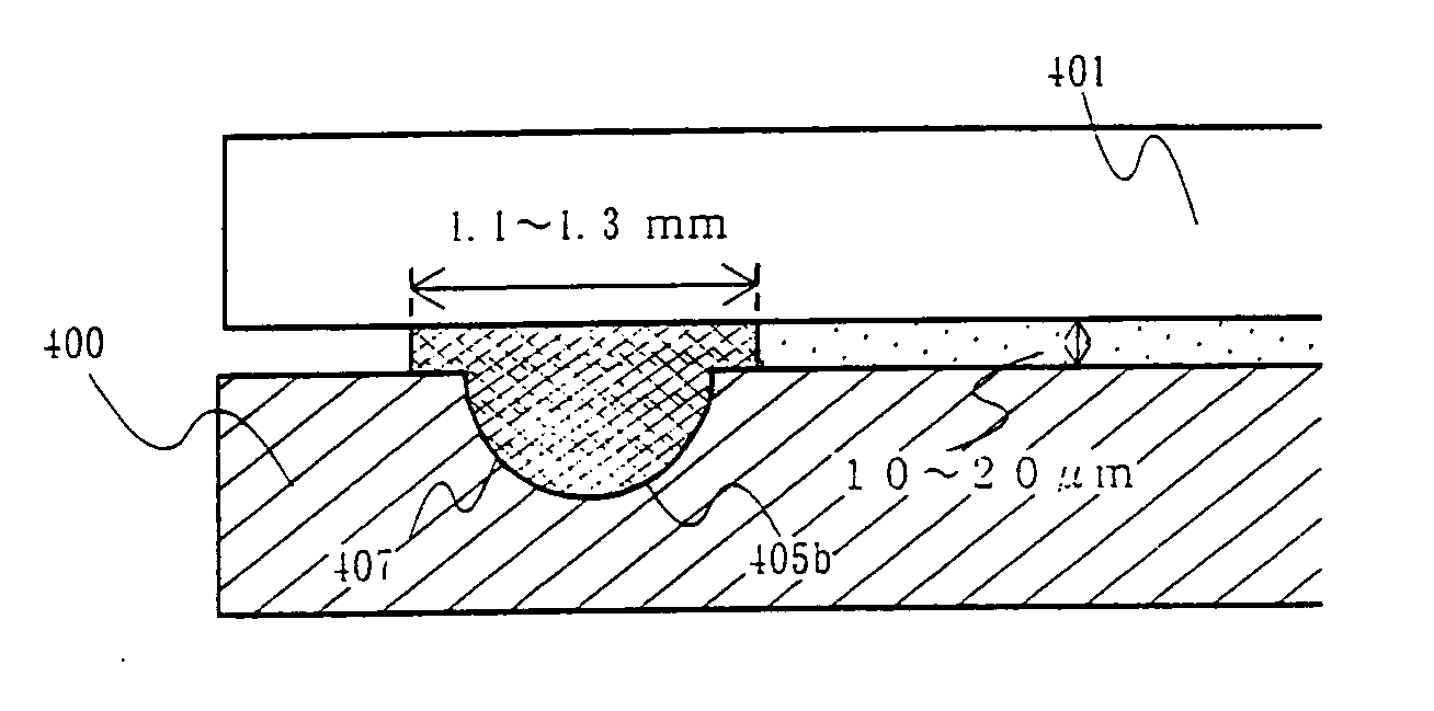
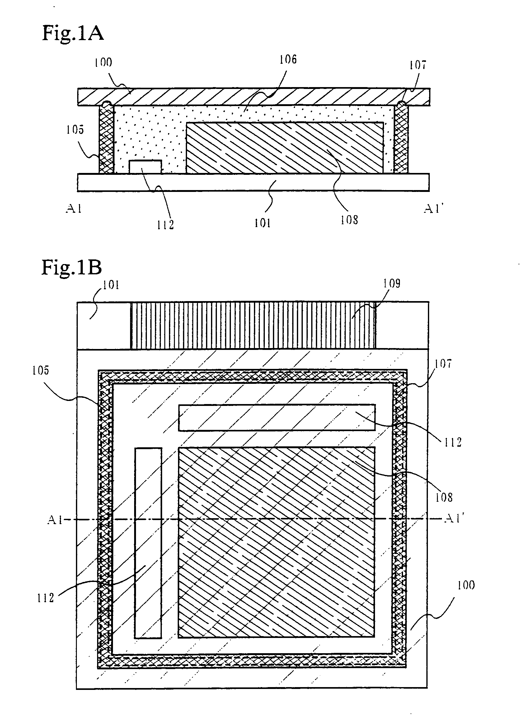
[0059] A light emitting device with lower surface emission, to which the present invention is applied, is shown in FIGS. 6A and 6B. The case, in which emitted light that passes through a first substrate 401, is referred to as “lower surface emission” in this specification. The direction of light is shown by an arrow. FIG. 6A is a cross sectional diagram of the light emitting device according to the present invention, cut along a dotted line segment A2-A2′ in FIG. 6B, and FIG. 6B is an upper surface diagram of the light emitting device according to the present invention.
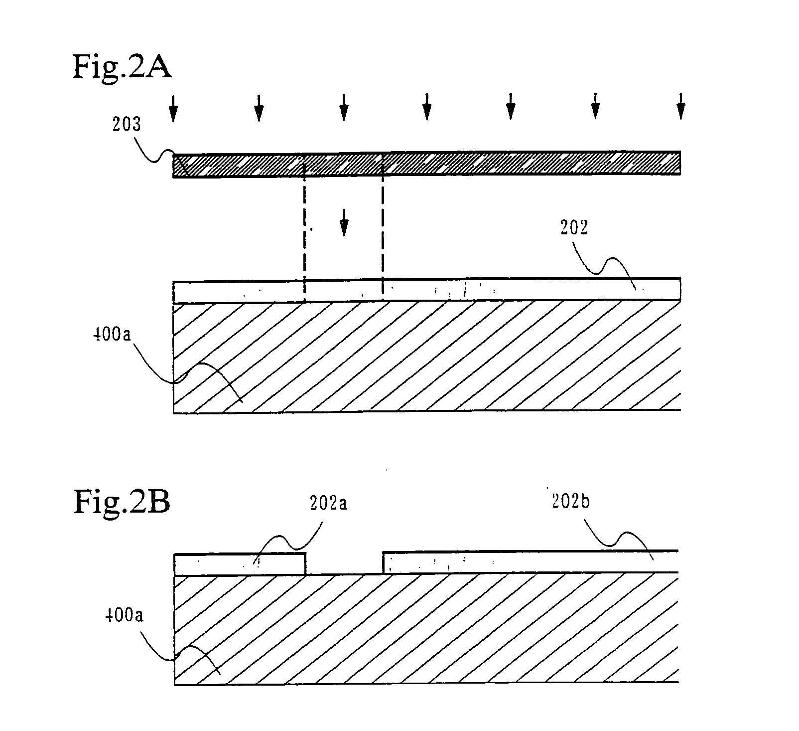
[0060] First, as shown in FIG. 2A, a resist 202 is formed by spin coating on a second substrate 400a made from glass. The resist 202 is then exposed to light using a mask 203 that can make a thinner resist pattern than the actual width of a seal pattern (resist application / exposure in FIG. 2A). Development is performed next as shown in FIG. 2B, and a portion of the resist for forming a concave portion is...
embodiment 2
[0071] Although a method of manufacturing a concave portion by etching of glass is discussed in Embodiment 1, a method of manufacturing a concave portion by sandblasting of glass is discussed in Embodiment 2. A method of manufacturing other parts of the device are the same as those of Embodiment 1, and a detailed explanation is thus omitted.
[0072] Resist is formed on portions of a glass substrate except a portion in which a concave portion is to be formed. The substrate is placed within a sandblast apparatus, and sand is blown onto the glass substrate. When the resist is then removed, a second substrate, in which a concave portion is formed by cutting glass out, is completed. A known sandblast apparatus may be used.
[0073] A light emitting element is formed next on a first substrate, on which a wiring portion and a driver circuit have been formed, and the first substrate and the second substrate on which the concave portion is formed, are bonded by using a sealing material. A light...
embodiment 3
[0074] Although a method of forming a concave portion by sandblasting of glass is discussed in Embodiment 2, a method of manufacturing glass by using a mold is discussed in Embodiment 3. A method of manufacturing other parts of the device are the same as those of Embodiment 1, and a detailed explanation is thus omitted.
[0075] A glass substrate with a concave portion is formed by a mold. A convex shape mold is formed so as to be able to form the concave portion in the glass substrate, and a second substrate, in which a concave portion is formed, is manufactured using the mold.
[0076] A light emitting element is formed next on a first substrate, on which a wiring portion and a driver circuit have been formed, and the first substrate and the second substrate on which the concave portion is formed, are bonded by using a sealing material. A light emitting device of the present invention is then completed by cutting the substrates into a desired size.
PUM
 Abstract
Description
Claims
Application Information