Circuit for power amplification

a power amplifier and circuit technology, applied in the direction of automatic tone/bandwidth control, high frequency amplifiers, gain control, etc., can solve the problems of reducing transmission power available, undesirable use of compensatory matching networks, and adversely affecting efficiency, so as to reduce circuit output power variation and mitigate problems.

Active Publication Date: 2006-03-30
TELEFON AB LM ERICSSON (PUBL)
View PDF8 Cites 82 Cited by
  • Summary
  • Abstract
  • Description
  • Claims
  • Application Information

AI Technical Summary

Benefits of technology

[0013] Advantageously, the present invention mitigates problems associated with output power control in the prior art. Also, low voltage transistors (and other low voltage technologies) can be used and the invention be implemented on an integrated circuit using a minimum of components. Where high output mismatch conditions result in the circuit experiencing a high VSWR, the present invention functions to reduce the circuit output power variation.
[0014] Further advantage is obtained in that both the driver transistor and output transistor are protected from excessive voltage levels.

Problems solved by technology

Unfortunately, many conventional antennas exhibit a high VSWR (for example, greater than 3:1) which adversely affects efficiency, especially in wideband antennas, unless some form of compensatory matching network is used.
Use of such compensatory matching networks is undesirable because they tend to decrease transmission power available and slow the operation of the system.
Substantially mismatched loads (and hence a high VSWR) can lead to a degradation of the RF power amplifier.
This degradation, or even transistor failure, occurs as a result of exceeding the collector-emitter voltage and collector current that can safely be applied to a bipolar transistor (here, the output transistor) within the constraints of the ‘secondary breakdown’ effect.
The output transistor is not able to draw d.c. current (as a capacitor is used to remove the d.c. component) and so the output bias circuitry provides increased bias current, which leads to increased input power to the output transistor.
Where a system is experiencing high VSWR and high load impedance, and hence a large voltage swing at the collector electrode of the output transistor, it is possible that negative gain can occur in the output amplifier.

Method used


Image

  • Circuit for power amplification
  • Circuit for power amplification
  • Circuit for power amplification

Examples


Embodiment Construction

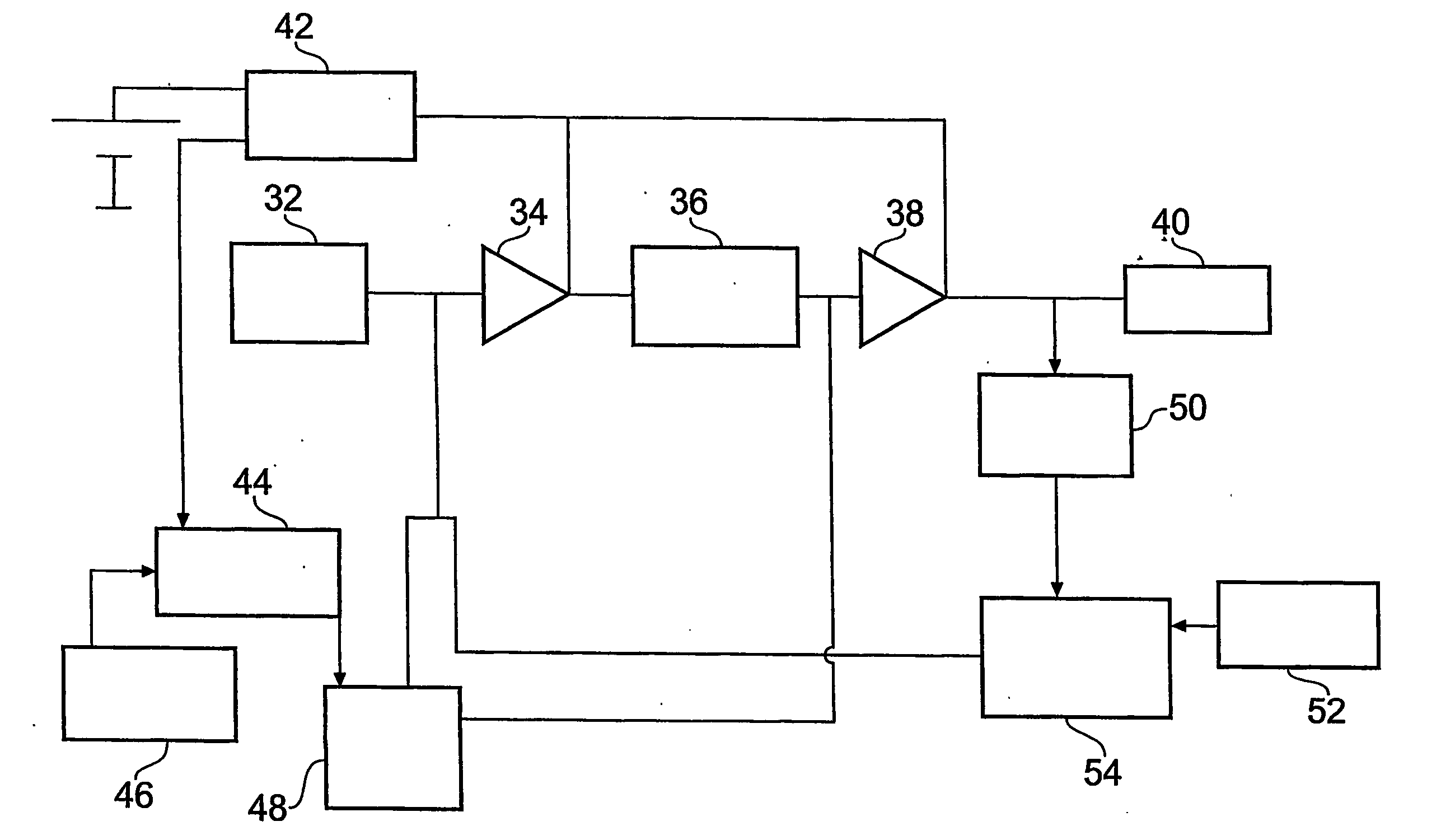
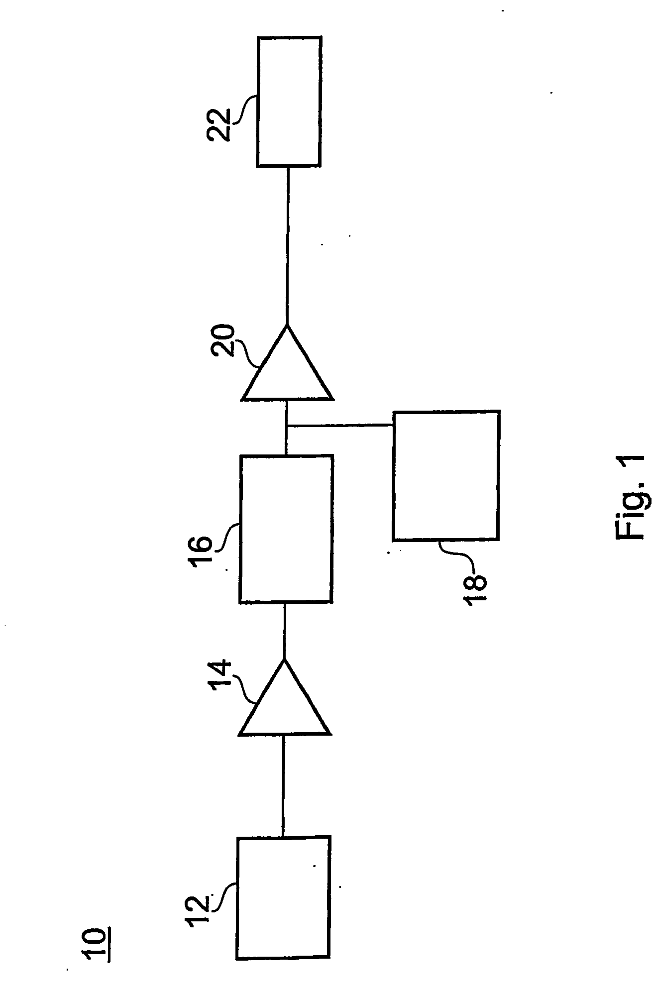
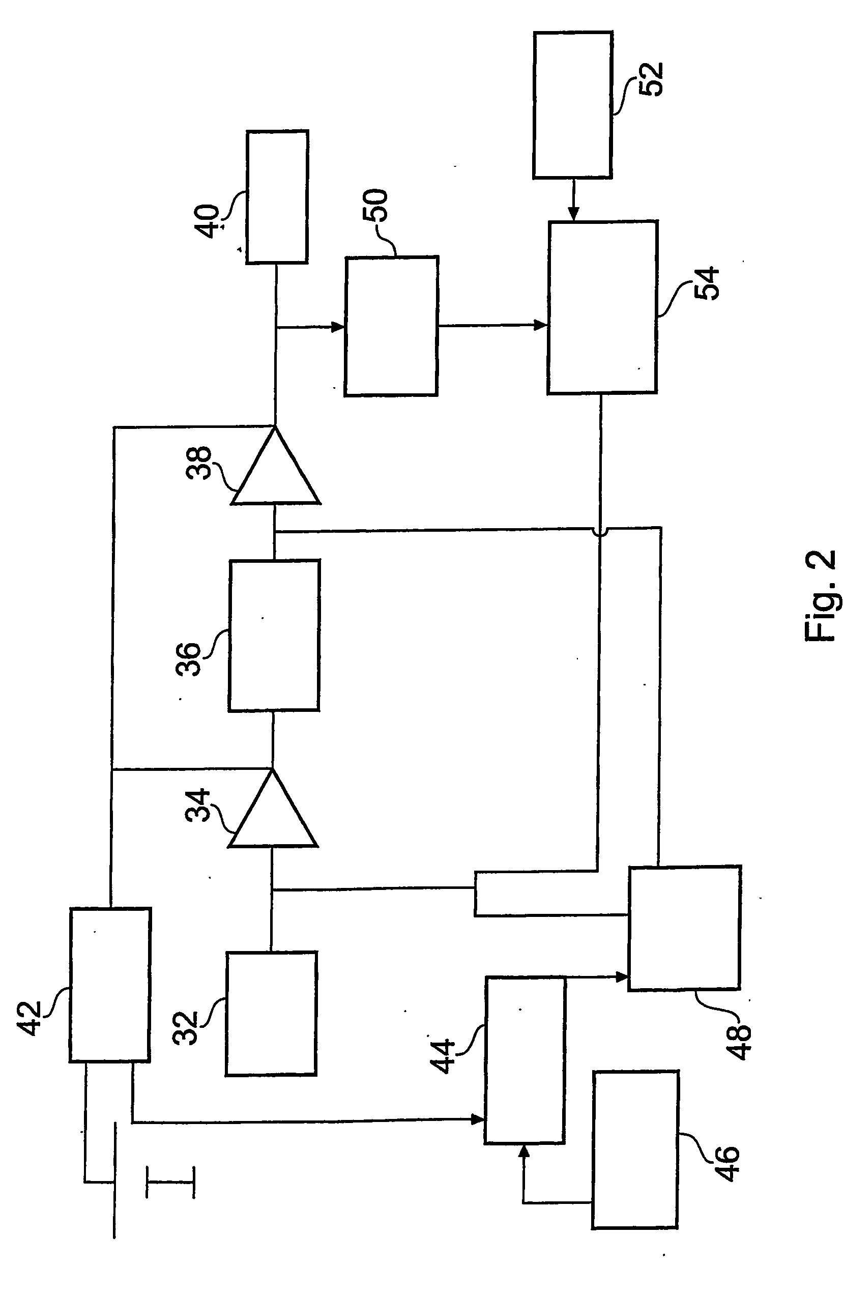
[0020]FIG. 1 illustrates a RF power amplifier 10, in which a RF signal 12 is input to a driver transistor 14. The collector electrode of the driver transistor 14 is coupled to a capacitor 16, which, in turn is coupled to an output transistor 20. An output bias circuitry 18 is coupled to the base electrode of the output transistor 20. Finally, the collector electrode of the output transistor 20 is coupled to a RF load 22. Generally, the RF load 22 is an antenna.

[0021] In operation, the RF signal 12 is amplified by the driver transistor 14, and the capacitor 16 serves to remove any d.c. component (leaving only the a.c. component) of the amplified signal before it is input to the output transistor 20. An approximately constant bias current is output from the output bias circuitry 18 and functions to bias the output transistor 20 such that the output transistor collector current is controlled.

[0022] The capacitor 16 functions to match impedance in the circuit and can be replaced by an...


PUM


Abstract

A radio frequency (RF) power amplifier, including an external control loop and a protection circuit, which functions to maintain a constant output power during variations in impedance on the RF load. In the external control loop a collector current from an output transistor is detected and then regulated with respect to a reference current. The regulated signal is utilised to generate a bias control signal which is input to the base electrode of both a driver transistor and the output transistor. The protection circuit detects a voltage envelope at the collector electrode of the output transistor and utilises this signal to form a bias reduction signal which is input to the base electrode of the driver transistor.

Description

TECHNICAL FIELD OF THE INVENTION [0001] The present invention relates to a power control circuit and method, and in particular to the control of output power of a high frequency power amplifier. DESCRIPTION OF THE RELATED ART [0002] In modern telecommunication systems, radio frequency (RF) power amplifiers are used to control output power of mobile devices (such as cellular telephones, cordless telephones, two-way pagers, wireless LAN, AM / FM analogue transmitters) prior to, and during, signal transmission. These RF power amplifiers typically generate an output power in the range of 50 mW to 3 W. Known RF power amplifiers can control output power at a RF load (which is generally an antenna) via biasing an output transistor. [0003] Generally in RF power amplifiers, impedance at the output transistor must match the nominal impedance of the load in order to avoid problems such as unwanted standing waves (resulting from signal reflection at the load) in the apparatus. Efficient antenna o...

Claims


Application Information

Patent Timeline
Patent Type & Authority Applications(United States)
IPC IPC(8): H03G3/20H03F1/02H03F1/52H03G3/30
CPCH03F1/0261H03F1/0272H03F1/52H03G3/3042H03F2200/102H03F2200/451H03F2200/99H03F3/19
Inventor BRANDT, PER-OLOF
Owner TELEFON AB LM ERICSSON (PUBL)
Why Eureka
Try Eureka