High frequency power amplifier circuit and electric component for high frequency power amplifier

Active Publication Date: 2006-03-30
MURATA MFG CO LTD
View PDF3 Cites 26 Cited by
  • Summary
  • Abstract
  • Description
  • Claims
  • Application Information

AI Technical Summary

Benefits of technology

[0012] It is an object of the present invention to enable preventing waveform distortion near the peak output power level by allowing sufficient idle currents to flow through the transistors for amplification, while enhancing the power efficiency in a low output power region in a high frequency power amplifier circuit in which bias application to the transistors for amplification is performed by current mirroring.
[0013] It is another object of the present invention to enable compact and high integration of a semiconductor integrated circuit for high frequency power amplification in which bias application to bipolar transistors for amplification is performed by current mirroring and an electronic component for high frequency power amplification (RF power module) in which the semiconductor integrated circuit for high frequency power amplification is installed.
[0017] According to this aspect, even if the bias voltages are constant, it is possible to allow an idle current fit for the level of an input high frequency signal to flow through the last-stage transistor for amplification. Thus, by allowing a sufficient idle current to flow through the last-stage transistor for amplification, waveform distortion near the peak output power level can be prevented. On the other hand, in a low output power region, the idle current flowing through the last-stage transistor for amplification can be reduced, so that power efficiency can be enhanced. Because diodes, capacitors, and a low-pass filter are not used, external elements are not necessary, and packaging constituent elements and circuits in a semiconductor integrated circuit is easy.
[0019] According to the present invention, in a high frequency power amplifier circuit in which biases are applied to the transistors for amplification by current mirroring, it is possible to prevent waveform distortion near the peak output power level by allowing sufficient idle currents to flow through the transistors for amplification and enhance power efficiency in a low output power region.
[0020] An advantage according to the present invention is providing the capability to realize compact and high integration of a semiconductor integrated circuit for high frequency power amplifier in which bias application to bipolar transistors for amplification is performed by current mirroring and an electronic component for high frequency power amplification (RF power module) in which the semiconductor integrated circuit for high frequency power amplification is installed.

Problems solved by technology

In the method of application of constant bias voltages to the transistors for amplification, however, it has been revealed that there is a problem of a decrease in power efficiency in a low region of output power because of the relatively large idle currents.
This poses a problem of difficulty in reducing the size of a module and a wireless communication system (mobile telephone).

Method used


Image

  • High frequency power amplifier circuit and electric component for high frequency power amplifier
  • High frequency power amplifier circuit and electric component for high frequency power amplifier
  • High frequency power amplifier circuit and electric component for high frequency power amplifier

Examples


first embodiment

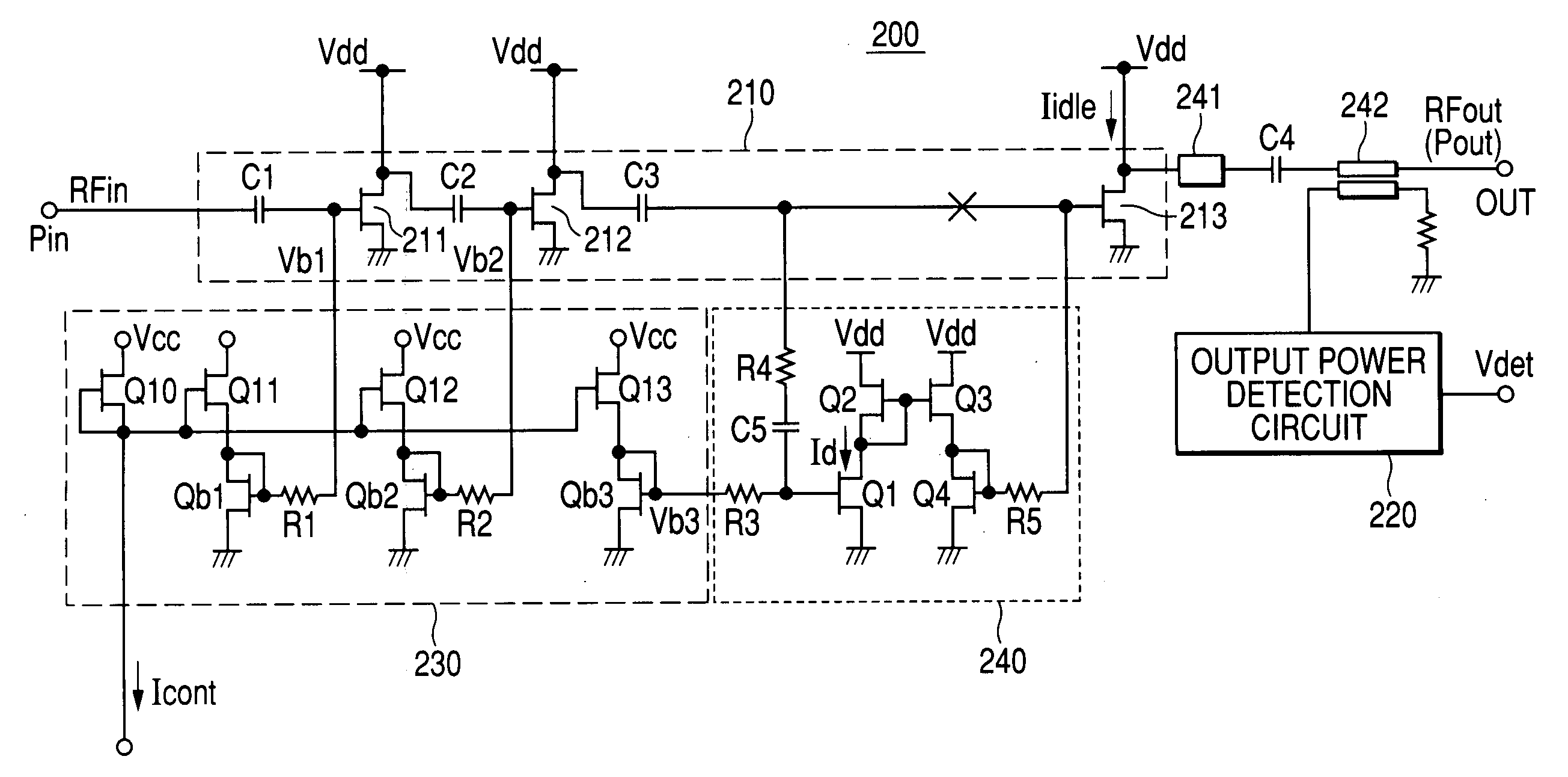
[0029]FIG. 1 shows a first embodiment of a high frequency power amplifier circuit to which the present invention is applied and a high frequency power amplification unit (hereinafter referred to as a power module) in which the above circuit is installed. In this specification, a structure in which a plurality of semiconductor chips and discrete components are installed on an insulating substrate like a ceramic substrate having printed wiring patterns on its surface and inside it and the components are interconnected by the printed wiring and bonding wires to perform their specific functions, wherein the structure is treated like a single electronic component, is called a module.

[0030] The power module 200 of this embodiment is comprised of a high frequency power amplifier block 210 including FETs for amplification which amplify an input high frequency signal RFin, an output power detection circuit 220 which detects the output power of the high frequency power amplifier block 210, a...

embodiment 2

[0055]FIG. 5 shows a second embodiment of a high frequency power amplifier circuit to which the present invention is applied and a power module in which the above circuit is installed. This embodiment is applied to a high frequency power amplifier circuit using an output power control method in which a drain voltage Vdd1 is controlled, while the gate biases of the transistors 211-213 for amplification are fixed. The amplitude of an input high frequency signal RFin is set constant.

[0056] As shown in FIG. 5, in this embodiment, inductors L1-L3 respectively connected to the drain terminals of the transistors 211-213 for amplification and a MOS transistor Q0 connected between the inductors L1-L3 and a supply voltage terminal Vdd, a differential amplifier AP which controls the gate voltage of the MOS transistor Q0 are provided. For the transistor Q0, a relatively large MOS transistor allowing for a relatively large current to flow is used. The differential amplifier AMP in which a contr...


PUM


Abstract

In a high frequency power amplifier circuit in which bias voltages are applied to the transistors for amplification by current mirroring, this invention enables preventing waveform distortion near the peak output power level by allowing sufficient idle currents to flow through the transistors for amplification, while enhancing the power efficiency in a low output power region. The power amplifier includes a detection circuit comprising a transistor for detection which receives the AC component of an input signal to the last-stage transistor for amplification at its control terminal, a current mirror circuit which mirrors current flowing through that transistor, and a current-voltage conversion means which converts current flowing in the slave side of the current mirror circuit into a voltage. In the detection circuit, a voltage from a bias circuit for generating the bias voltages for the transistors for amplification is applied to the control terminal of the transistor for detection and output of the detection circuit is applied to the control terminal of the last-stage transistor for amplification.

Description

CROSS-REFERENCE TO RELATED APPLICATION [0001] The present application claims priority from Japanese patent application No. 2004-276261 filed on Sep. 24, 2004, the content of which is hereby incorporated by reference into this application. BACKGROUND OF THE INVENTION [0002] The present invention relates to a technique that is effective for application to a high frequency power amplifier circuit and an electronic component for high frequency power amplification (RF power module) in which the high frequency power amplifier circuit is installed. More particularly, the invention relates to a technique for enhancing the power efficiency of a high frequency power amplifier circuit in which bias application to transistors for amplification is performed by current mirroring. [0003] A high frequency power amplifier circuit (usually consisting of multiple stages) employing semiconductor elements such as MOSFETs (insulated gate type field effect transistors) and GaAs-MESFETs for power amplifica...

Claims


Application Information

Patent Timeline
IPC IPC(8): H03G3/20
CPCH03F1/30H03F1/32H03F3/191H03G1/007H03G2201/40H03G3/3047H03G2201/103H03G2201/206H03G2201/307H03G3/004
Inventor AKAMINE, HITOSHITSUCHIYA, MASAHIROTAKAHASHI, KYOICHIKOSHIO, KAZUHIRO
Owner MURATA MFG CO LTD
Why Eureka
Try Eureka