Integrated diode in a silicon chip scale package

a silicon chip scale and integrated diode technology, applied in the field of optical transmitters, can solve the problems of limited data capacity of copper wire based cables, less attractive as a solution for many modern networks, and current designs suffer from several drawbacks, and achieve the effect of more surface area

Active Publication Date: 2006-04-06
II VI DELAWARE INC
View PDF14 Cites 31 Cited by
  • Summary
  • Abstract
  • Description
  • Claims
  • Application Information

AI Technical Summary

Benefits of technology

[0017] Advantageously, the embodiments described above include large back monitor photodiodes to provide for more surface area where optical energy can be sensed. Additionally, the sloped trench walls help to direct light energy into the photodiodes. Alternatively, the embodiments summarized above may be used to integrate a protection diode in the same structure as an optical source. This allows for manufacturing optical sources with integrated ESD protection.

Problems solved by technology

However, copper wire based cables are subject to limitations that are making them less attractive as a solution for many modern networks.
Specifically, the copper wire based cables are limited in the amount of data they can carry in a given time period and the length that the data can travel.
Unfortunately, current designs suffer from several drawbacks.
For example, the use of discrete components results in inconsistencies in how the back monitor photodiode receives optical power.
Further, packaging and / or other external elements that reflect light are typically not configured to reflect light into a back monitor photodiode.
Thus, any power reflected back into the back monitor photodiode is not regulated or controlled and in some environments is at least partially random.
Another challenge that is experienced in laser devices such as Vertical Cavity Surface Emitting Lasers (VCSELs) relates to Electrostatic Discharge (ESD) damage.
Exposure to ESDs is one very common cause of VCSEL failure.
Further, the smaller an aperture of emission in the VCSEL, the lower the amount of ESD voltage a VCSEL can withstand.
As an example, a VCSEL with a aperture diameter of about 5 microns may be damaged when ESD levels are on the order of about 100V using a human ESD model.
However, using external components significantly increases the total size of packaging needed.
This may be less desirable when there is a need or advantage to having smaller component packaging.

Method used


Image

  • Integrated diode in a silicon chip scale package
  • Integrated diode in a silicon chip scale package
  • Integrated diode in a silicon chip scale package

Examples


Embodiment Construction

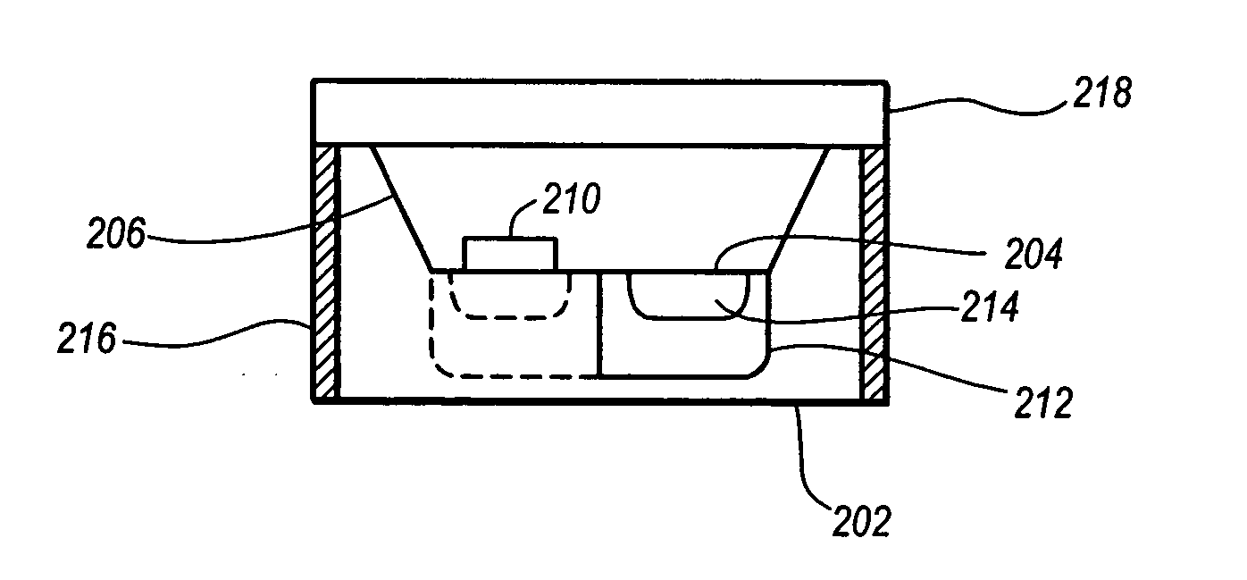
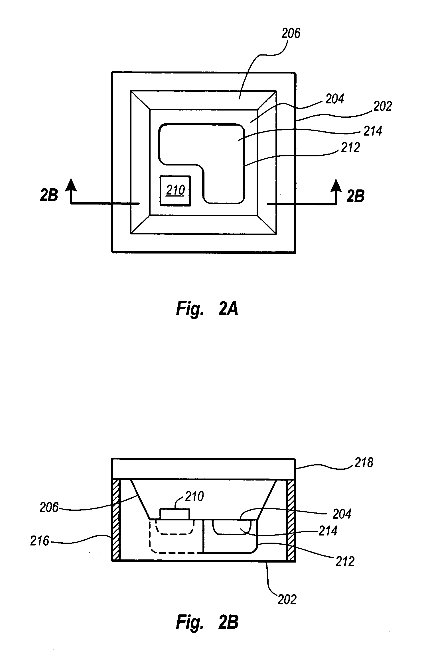
[0023] One embodiment described herein relates to an optical source, such as a laser diode or LED, which is formed in a package that may also include a back monitor photodiode or an integrated protection diode. Specifically, the package is formed from a semiconductor substrate. A sloped wall trench formed in the semiconductor substrate using an etching process. An optical source is placed in the trench either as a discrete component or through an epitaxial process. A back monitor photodiode is formed around the optical source in the trench or on the underside of the substrate. A protection diode may be formed in the substrate. The protection diode may be formed under the optical source, or in any other convenient location. The protection diode does not need to be formed such that it receives any reflected or otherwise transmitted light from the optical source.

[0024] In one embodiment, the semiconductor substrate is an n-type material, and the back monitor photodiode or protection d...


PUM


Abstract

An optical component with integrated back monitor photodiode. The optical component includes a substrate doped with a first type dopant, such as an n-type dopant. The substrate has a trench with sloped walls. An optical source is disposed in the trench. An implant of a second type dopant, such as a p-type dopant, is in the substrate around at a least a portion of the optical source. The implant in the substrate in combination with the first type dopant in the substrate forms a diode.

Description

CROSS-REFERENCE TO RELATED APPLICATIONS [0001] This application claims the benefit of U.S. Provisional Application No. 60 / 615,474, titled “Integrated Back Monitor Photodiode In a Silicon Ship Scale Package” filed Oct. 1, 2004, which is incorporated herein by reference.BACKGROUND OF THE INVENTION [0002] 1. The Field of the Invention [0003] The invention generally relates to the field of optical transmitters. More specifically, the invention relates to optical transmitters packaged with integrated diodes. [0004] 2. Description of the Related Art [0005] Modern day computer networks allow for transmissions of large amounts of data between computer terminals. Data may be transmitted on a network across a number of different mediums. For example, data may be transmitted across traditional copper wire based cables. However, copper wire based cables are subject to limitations that are making them less attractive as a solution for many modern networks. Specifically, the copper wire based cab...

Claims


Application Information

Patent Timeline
Patent Type & Authority Applications(United States)
IPC IPC(8): H01L33/00
CPCH01L25/167H01L2924/3011H01S5/005H01S5/0201H01S5/0261H01S5/0264H01S5/06825H01L2224/45147H01L2924/00H01L2924/10253H01L2924/01015H01L2924/00014H01L2224/48
Inventor GUENTER, JAMES K.
Owner II VI DELAWARE INC
Why Eureka
Try Eureka