Semiconductor light emitting device

a technology of semiconductors and light emitting devices, applied in the direction of discharge tubes/lamp details, discharge tubes luminescnet screens, coatings, etc., can solve the problems of color tone variation of products, decreased production yield, and unstable color tone response, and achieve the effect of small grain siz

Active Publication Date: 2006-04-06
SEOUL SEMICONDUCTOR
View PDF3 Cites 41 Cited by
  • Summary
  • Abstract
  • Description
  • Claims
  • Application Information

AI Technical Summary

Benefits of technology

[0027] at least one kind of phosphors of the at least two kinds of phosphors having a surface on which fine powder is attached, and being dispersed in the sealing resin, the fine powder being made of material different from and having a smaller grain size than both the at least two kinds of phosphors.

Problems solved by technology

This causes a problem that various factors in the manufacturing process lead to the color tone variation of products and the decrease of production yield.
In this case, however, there is a problem that the color tone is unstable in response to the variation of ambient temperature because the temperature dependence of light emission in the light emitting element is different from the temperature dependence of wavelength conversion in the phosphors.
Moreover, the combination of a semiconductor light emitting element and a single kind of phosphors is also unfavorable because the achievable color range is limited to composites of the two colors.

Method used


Image

  • Semiconductor light emitting device
  • Semiconductor light emitting device
  • Semiconductor light emitting device

Examples


first embodiment

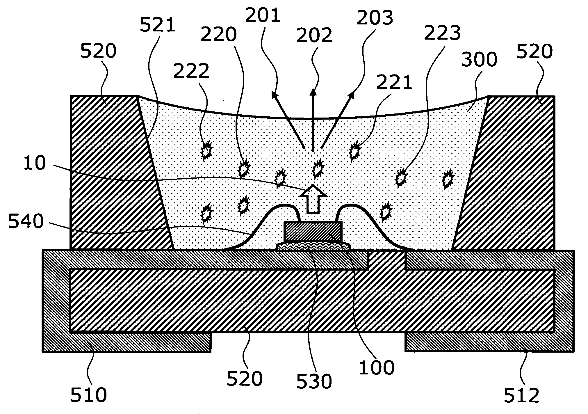
[0041]FIG. 1 is a schematic cross section illustrating the structure of a relevant part of a semiconductor light emitting device according to the invention.

[0042] More specifically, the semiconductor light emitting device of this embodiment is of a type of surface mounted device (SMD) suitable to high density packaging on a mounting board. A semiconductor light emitting element 100 is bonded onto a first lead 510 using an adhesive 530. A first electrode provided on the upper face of the semiconductor light emitting element 100 is connected to the first lead 510 via a bonding wire 540. A second electrode provided on the upper face of the semiconductor light emitting element 100 is connected to a second lead 512 via a bonding wire. The leads 510 and 512, in the state of being connected onto a lead frame in advance, are embedded and fixed in thermoplastic resin 520 by injection molding or the like. Photoreflective material can be mixed in the thermoplastic resin 520 to form a photorefl...

second embodiment

[0085] Next, the invention is described.

[0086]FIG. 10A is a schematic cross section illustrating the structure of a relevant part of a semiconductor light emitting device according to a second embodiment of the invention. FIG. 10B is an enlarged schematic cross section of the phosphors.

[0087] With regard to these figures again, elements similar to those described above with reference to FIGS. 1 to 9 are marked with the same reference numerals and will not be described in detail.

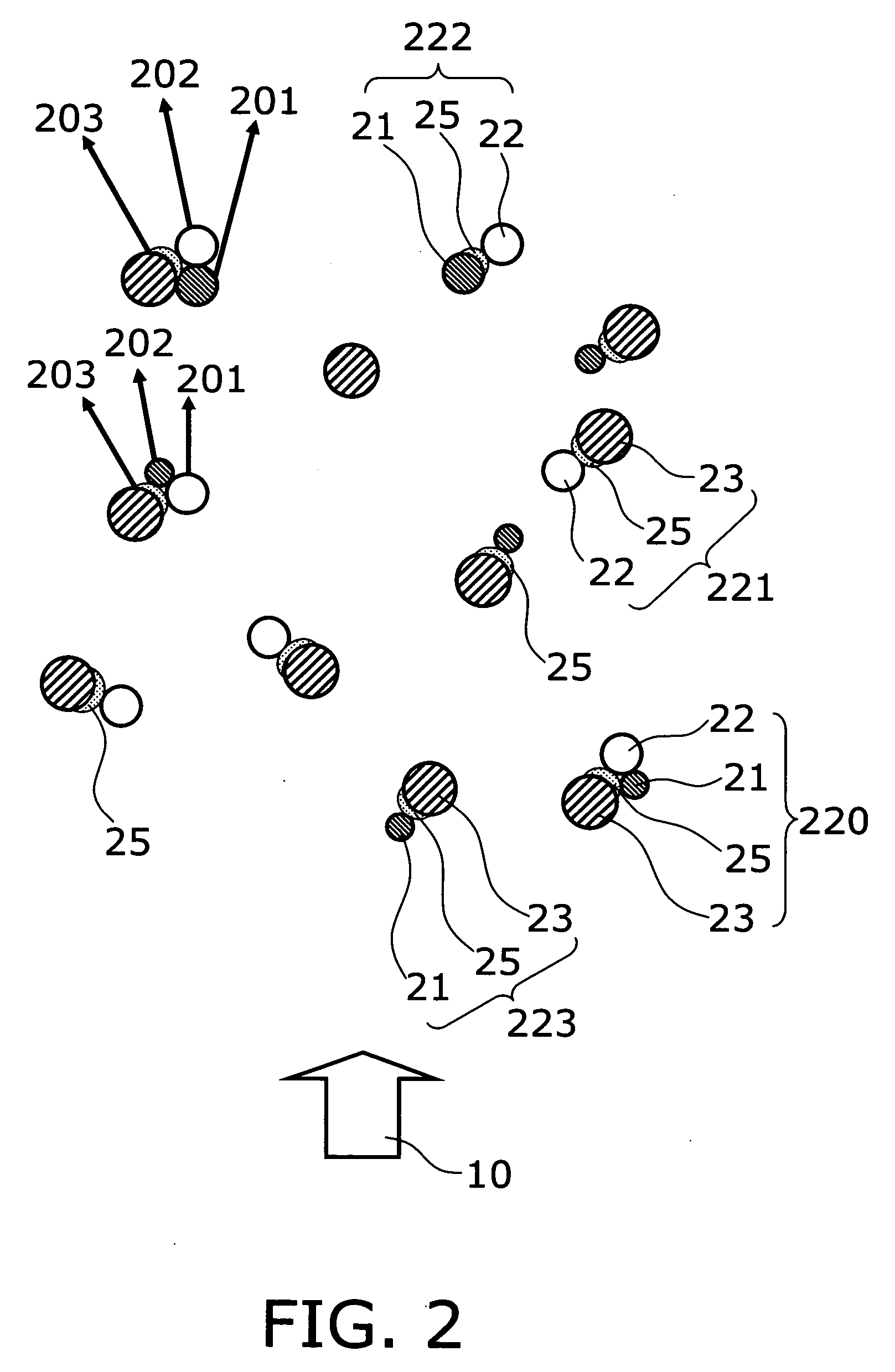
[0088] In this embodiment, transparent fine powder 210 is attached to the surface of the phosphors (e.g., red phosphors 23) being likely to sediment, among several kinds of phosphors (e.g., blue phosphors 21, green phosphors 22, and red phosphors 23), thereby forming powder-attached phosphors 230. The transparent fine powder 210 is made of material different from the phosphor 23, and has a smaller grain size than the phosphor 23. The transparent fine powder 210 may be made of, for example, material having g...


PUM

PropertyMeasurementUnit
grain sizeaaaaaaaaaa
wavelength bandaaaaaaaaaa

Abstract

A semiconductor light emitting device comprises: a semiconductor light emitting element that emits light of a first wavelength; at least two kinds of phosphors that absorb the light of the first wavelength and then emit wavelength-converted light; sealing resin in which the at least two kinds of phosphors are dispersed and the semiconductor light emitting element is embedded; and binder resin. Combined bodies in which the at least two kinds of phosphors are combined by the binder resin are dispersed in the sealing resin.

Description

CROSS-REFERENCE TO RELATED APPLICATIONS [0001] This application is based upon and claims the benefit of priority from the prior Japanese Patent Application No. 2004-255809, filed on Sep. 2, 2004; the entire contents of which are incorporated herein by reference. BACKGROUND OF THE INVENTION [0002] 1. Field of the Invention [0003] This invention relates to a semiconductor light emitting device based on a semiconductor light emitting element such as a light emitting diode (LED), and more particularly to a semiconductor light emitting device for use in a white light source including a semiconductor light emitting element combined with phosphors. [0004] 2. Background Art [0005] In recent years, semiconductor light emitting devices have been widely used for various light sources including illumination and display devices. In particular, realization of blue light emitting elements and ultraviolet elements made of GaN-based material has dramatically extended the application of white light e...

Claims


Application Information

Patent Timeline
Patent Type & Authority Applications(United States)
IPC IPC(8): H01J1/62H01L33/50H01L33/60H01L33/62
CPCB29C45/0013B29C45/14655H01L33/504H01L2224/32245H01L2224/48091H01L2224/48247H01L2224/73265H01L2924/00014H01L2924/00H01L2924/181
Inventor TAKEZAWA, HATSUOSHIMOMURA, KENJIOSHIO, HIROAKISHIRAKAWA, YASUHIROISHII, TSUTOMU
Owner SEOUL SEMICONDUCTOR
Why Eureka
Try Eureka