

Pre-process before cutting a wafer and method of cutting a wafer
- Summary
- Abstract
- Description
- Claims
- Application Information
AI Technical Summary
Benefits of technology
Problems solved by technology
Method used
Image

Examples
Embodiment Construction
[0024] Reference will now be made in detail to the present preferred embodiments of the invention, examples of which are illustrated in the accompanying drawings. Wherever possible, the same reference numbers are used in the drawings and the description to refer to the same or like parts.
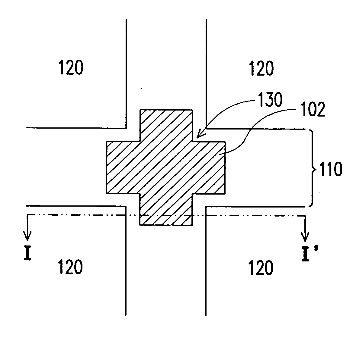
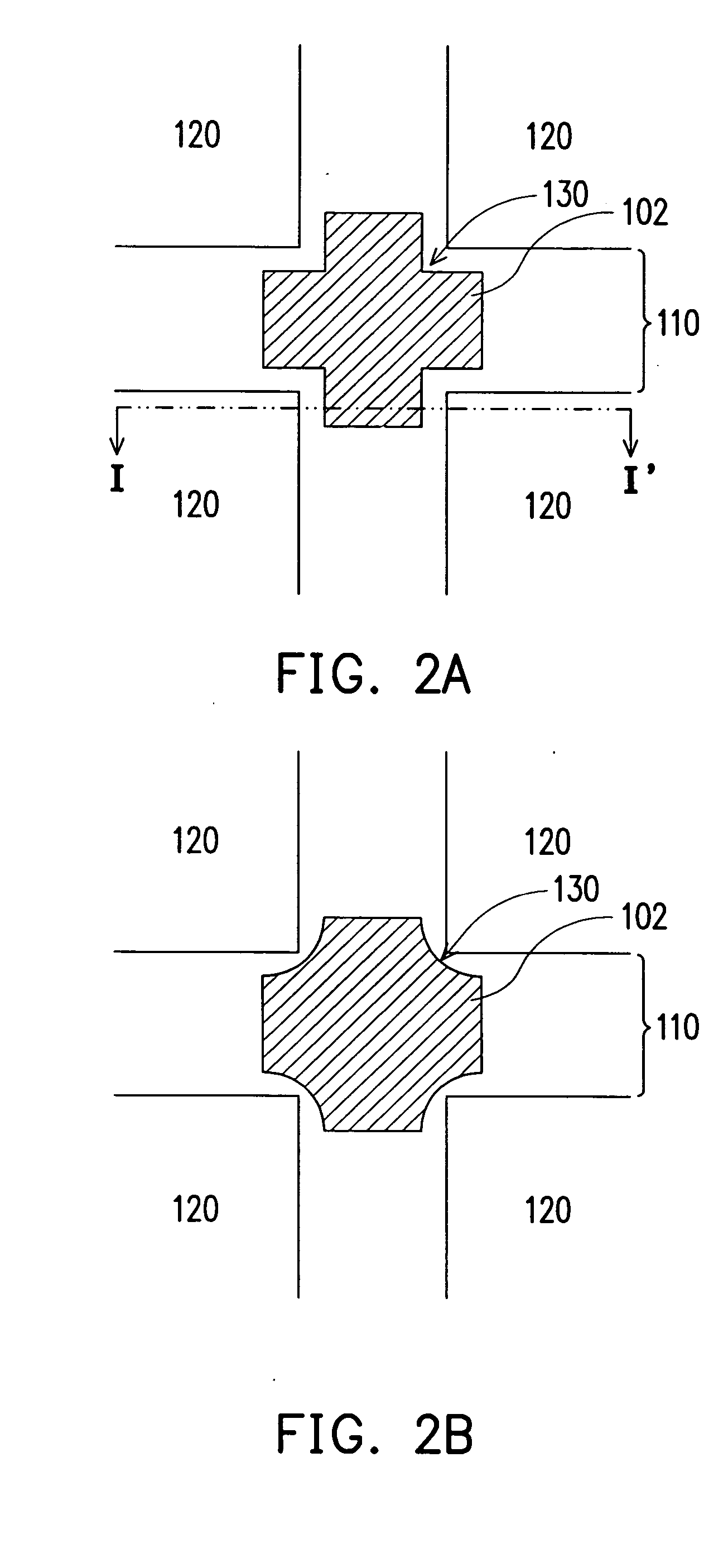
[0025] Typically, the devices on a wafer have a multi-layered structure. In the process of fabricating these devices, the same material layers are also formed on the scribe lines. When the wafer is cut to form independent dies, the material layers on the scribe lines may crack, peel of chip because of the difference in properties between the layers. Damages are particularly serious at the corner regions of the dies close to the cross-junction of the scribe lines because these are the areas where stresses are concentrated.
[0026] To combat such damages, the present invention provides a pre-processing step before cutting the wafer. In the pre-processing step, the material layer on the scribe line clo...
PUM
 Abstract
Description
Claims
Application Information