Gas dielectric structure forming methods

Inactive Publication Date: 2006-04-06
GLOBALFOUNDRIES INC
View PDF19 Cites 93 Cited by
  • Summary
  • Abstract
  • Description
  • Claims
  • Application Information

AI Technical Summary

Benefits of technology

[0008] The invention includes methods of forming a gas dielectric structure for a semiconductor structure by using a sacrificial layer. In particular, one embodiment of the invention includes forming an opening for semiconductor structure in a dielectric layer on a substrate; depositing a sacrificial layer over the opening; performing a directional etch on the sacrificial layer to form a sacrific

Problems solved by technology

Unfortunately, as semiconductor device size is decreased, the capacitive coupling between conductors in a circuit tends to increase since the capacitive coupling is inversely proportional to the distance between the conductors.
This coupling may ultimately limit the speed of the chip or otherwise inhibit proper chip operation if steps are not taken to reduce the capacitive coupling.
One challenge facing further development is finding materials with a lower dielectric constant that can be used between the conductors.
Unfortunately, provision of newer low-k dielectric m

Method used


Image

  • Gas dielectric structure forming methods
  • Gas dielectric structure forming methods
  • Gas dielectric structure forming methods

Examples


Example

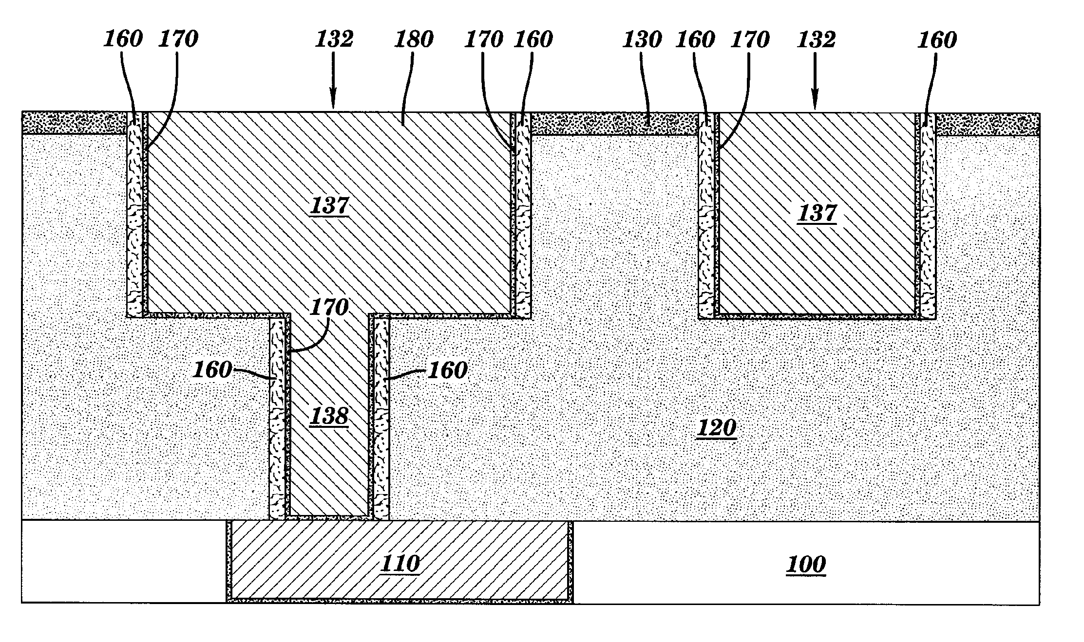
[0017] Referring to FIGS. 1-9, methods of forming a gas dielectric structure for a semiconductor structure will now be described.

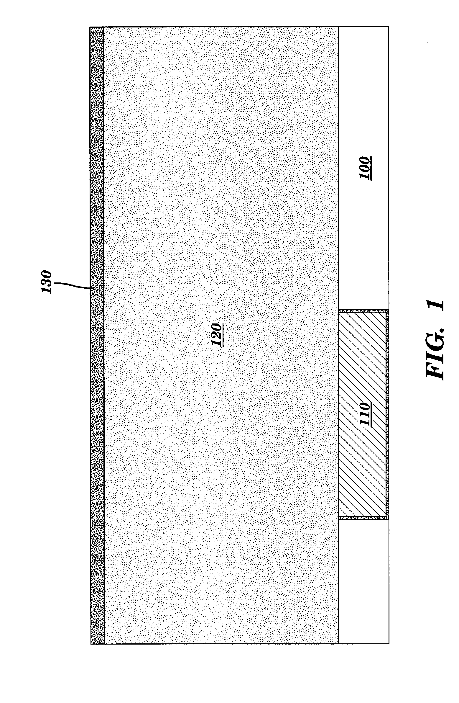
[0018] As shown in FIG. 1, a substrate 100, e.g., bulk silicon or silicon-on-insulator (SOI), with any typical conductor line 110 or active area, etc., patterned therein is provided. A dielectric layer 120 is also deposited thereon. Dielectric layer 120 can include any of numerous dielectric materials including but not limited to: silicon dioxide (SiO2), fluorinated SiO2, Silk™ available from Dow, SiCOH (carbon-doped oxide), Black Diamond™ available from Applied Materials, etc. A hard mask layer 130 can also be deposited on top of dielectric layer 120. Hard mask layer 130 can include any of numerous hard masks including but not limited to: SiO2, silicon nitride (SiN), oxynitride, blok, n-blok, etc.

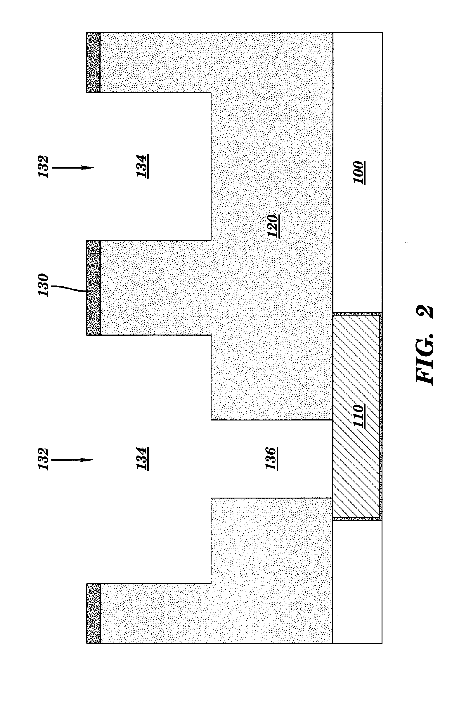
[0019] As shown in FIG. 2, a first step includes forming an opening 132 for a semiconductor structure in dielectric layer 120 on substrate 100. As illustrated,...


PUM


Abstract

Methods of forming a gas dielectric structure for a semiconductor structure by using a sacrificial layer. In particular, one embodiment of the invention includes forming an opening for semiconductor structure in a dielectric layer on a substrate; depositing a sacrificial layer over the opening; performing a directional etch on the sacrificial layer to form a sacrificial layer sidewall on the opening; depositing a conductive liner over the opening; depositing a metal in the opening; planarizing the metal and the conductive liner; removing the sacrificial layer sidewall to form a void; and depositing a cap layer over the void to form the gas dielectric structure. The invention is easily implemented in damascene wire formation processes, and improves structural stability.

Description

BACKGROUND OF THE INVENTION [0001] 1. Technical Field [0002] The present invention relates generally to semiconductor structures, and more particularly, to methods of forming a gas dielectric structure for a semiconductor structure. [0003] 2. Related Art [0004] In order to enhance semiconductor chip operational speed, semiconductor devices have been continuously scaled down in size. Unfortunately, as semiconductor device size is decreased, the capacitive coupling between conductors in a circuit tends to increase since the capacitive coupling is inversely proportional to the distance between the conductors. This coupling may ultimately limit the speed of the chip or otherwise inhibit proper chip operation if steps are not taken to reduce the capacitive coupling. [0005] The capacitance between conductors is also dependent on the insulator, or dielectric, used to separate the conductors. Traditional semiconductor fabrication commonly employs silicon dioxide (SiO2) as a dielectric, whic...

Claims


Application Information

Patent Timeline
IPC IPC(8): H01L21/4763H01L21/311
CPCH01L21/76807H01L21/7682H01L21/76831H01L23/5222H01L23/53223H01L23/53238H01L2924/0002H01L23/53252H01L23/53295H01L2924/00H01L2221/1063
Inventor FILIPPI, RONALD G.IGGULDEN, ROY C.KIEWRA, EDWARD W.WANG, PING-CHUAN
Owner GLOBALFOUNDRIES INC
Why Eureka
Try Eureka