
Eureka
For R&D, Eureka makes reading and utilizing patents & technical documents easy.
Eureka AIR
Designed for self-driven R&D workflows. Generate viable solutions, solve complex R&D challenges, empower your innovation with AI.

Eureka Materials
Designed for material experts only. Revolutionize your material R&D, from search, analyze, to developing new materials.

TechResearch
Generate reliable direction feasibility study reports for your R&D in just a few steps.

TechSeek
Discover and master advanced knowledge NOW. Basics, ideas, possibilities, all at once.

TechMind
As an expert in R&D Theories, TechMind can generates customized viable solutions instantly.

TechRisk
Analyze your overall solution with one click, know your potential R&D risks in advance.

TechMonitor
Get weekly tech updates, stay abreast of the latest tech innovations and key insights.
Semiconductor device and manufacturing method thereof
- Summary
- Abstract
- Description
- Claims
- Application Information
AI Technical Summary
Problems solved by technology
Method used
Image

Examples
Embodiment Construction
[0029] Next, a semiconductor device and its manufacturing method according to an embodiment of this invention will be explained, referring to FIGS. 1 through 7.
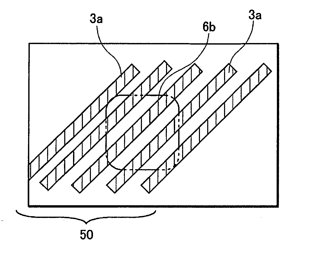
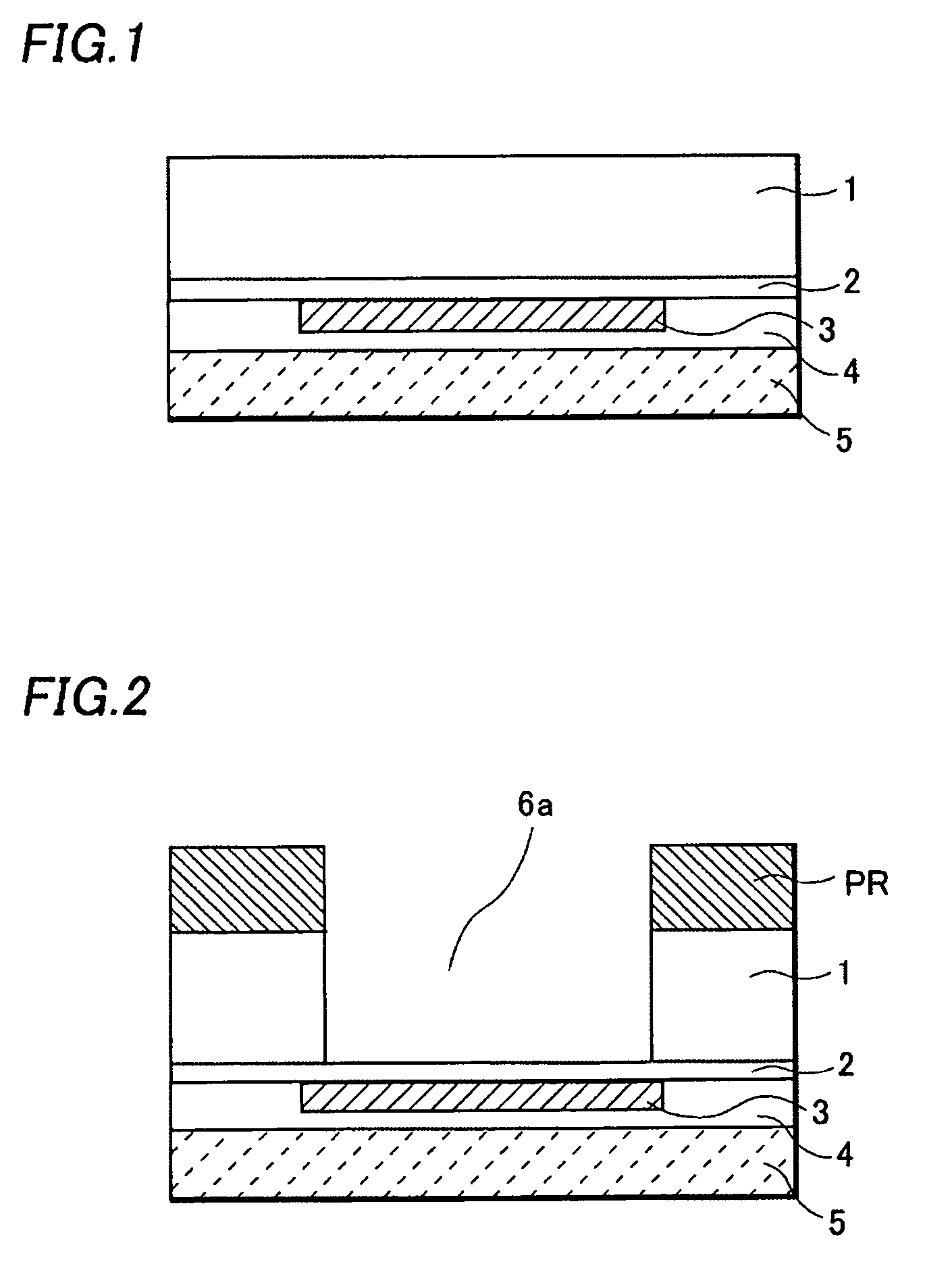
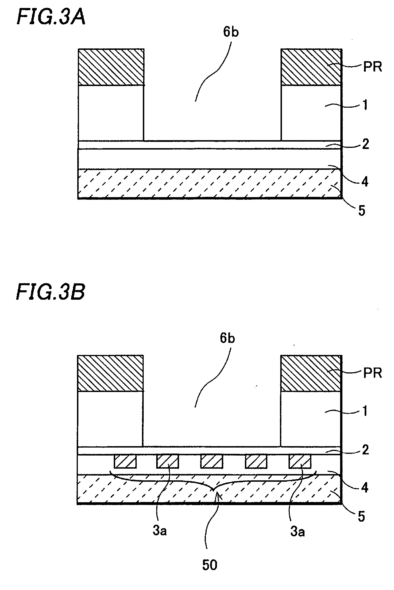
[0030] First, a pad electrode 3 made of a metal layer primarily composed of aluminum is formed on a front surface of a semiconductor substrate 1 through an insulation layer 2 made of a silicon oxide film or a silicon nitride film, as shown in FIG. 1. Then a supporting member 5 made of a glass substrate, for example, is bonded to the front surface of the semiconductor substrate 1 having the pad electrode 3 through an adhesive material 4 made of an epoxy resin layer. The silicon wafer in this embodiment is divided into individual silicon dice to form CCD (Charge Coupled Device) image sensor chips, for example. Because the CCD in the front surface of the silicon die needs to receive external light, the supporting member 5 is required to be made of a transparent substrate such as the glass substrate or a semi-transparent substra...
PUM
 Abstract
Description
Claims
Application Information
 - R&D Engineer
- R&D Manager
- IP Professional
- Industry Leading Data Capabilities
- Powerful AI technology
- Patent DNA Extraction
Browse by: Latest US Patents, China's latest patents, Technical Efficacy Thesaurus, Application Domain, Technology Topic, Popular Technical Reports.
© 2024 PatSnap. All rights reserved.Legal|Privacy policy|Modern Slavery Act Transparency Statement|Sitemap|About US| Contact US: help@patsnap.com