Apparatus and method for plasma assisted deposition

a technology of plasma assisted deposition and apparatus, which is applied in the direction of chemical vapor deposition coating, coating, electric discharge tube, etc., can solve the problems of easy recombined species, large amount of ongoing effort, and many traditional deposition processes that have difficulty filling sub-micron structures, etc., to achieve plasma-enhanced chemical vapor deposition.

Inactive Publication Date: 2006-04-13
APPLIED MATERIALS INC
View PDF99 Cites 153 Cited by
  • Summary
  • Abstract
  • Description
  • Claims
  • Application Information

AI Technical Summary

Problems solved by technology

However, as the fringes of circuit technology are pressed, the shrinking dimensions of interconnects in VLSI and ULSI technology have placed additional demands on the processing capabilities.
Many traditional deposition processes have difficulty filling sub-micron structures.
Therefore, there is a great amount of ongoing effort being directed at the formation of substantially void-free and seam-free sub-micron features having high aspect ratios.
One problem with the use of prior chambers, such as chamber 10, for atomic layer deposition requiring a plasma 80 is that the plasma 80 may etch or remove deposited materials on the surface of the substrate 36 due to the ion bombardment or sputtering by the plasma 80 of the deposited material on the substrate 36 which is particularly detrimental in atomic layer deposition in which a monolayer of material is desired to be deposited per cycle of gases.
One problem associated with these prior attempts is that the atomic species may easily recombine preventing the reaction of the atomic species on the surface of the substrate.

Method used


Image

  • Apparatus and method for plasma assisted deposition
  • Apparatus and method for plasma assisted deposition
  • Apparatus and method for plasma assisted deposition

Examples


Embodiment Construction

Process Chambers

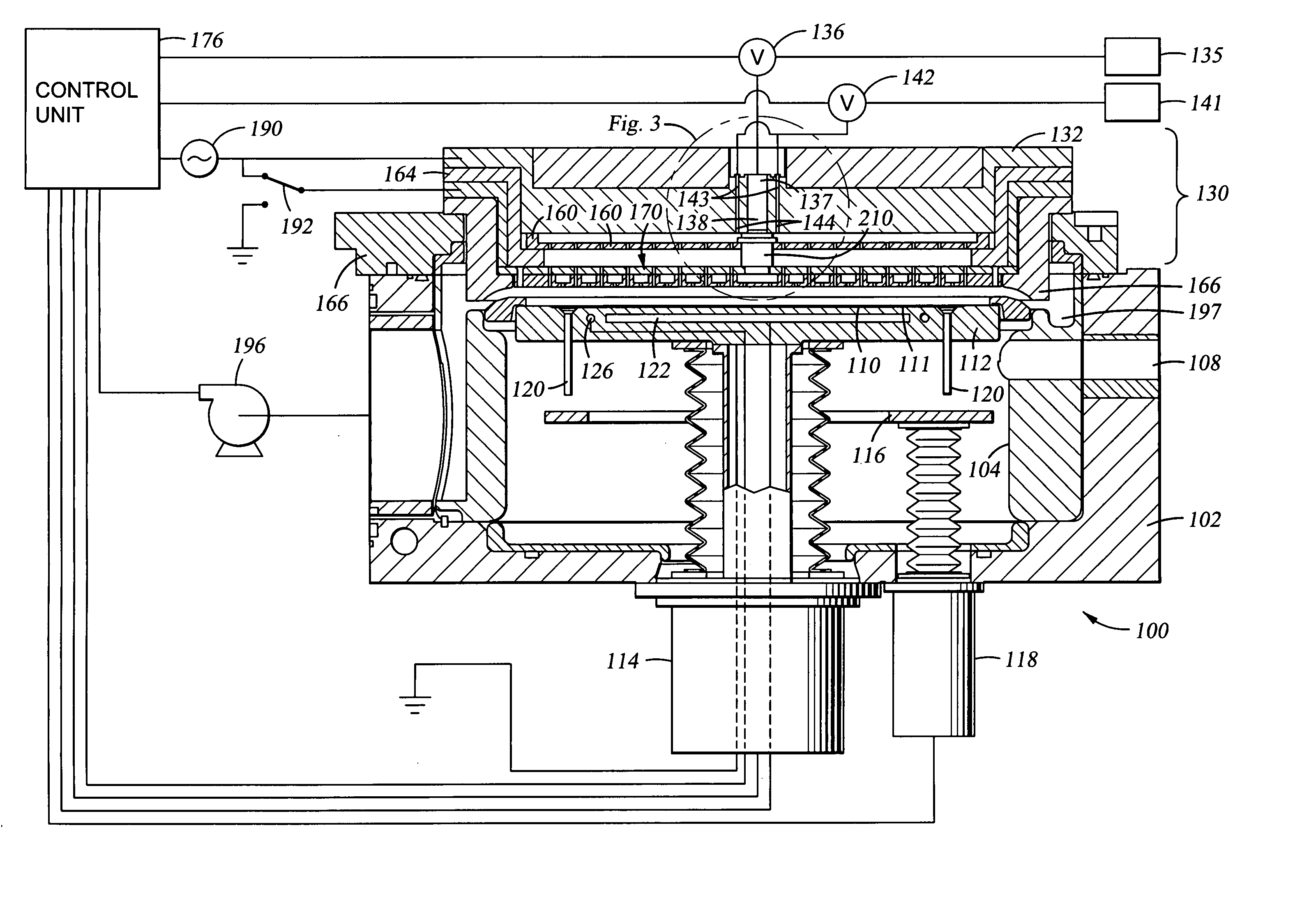
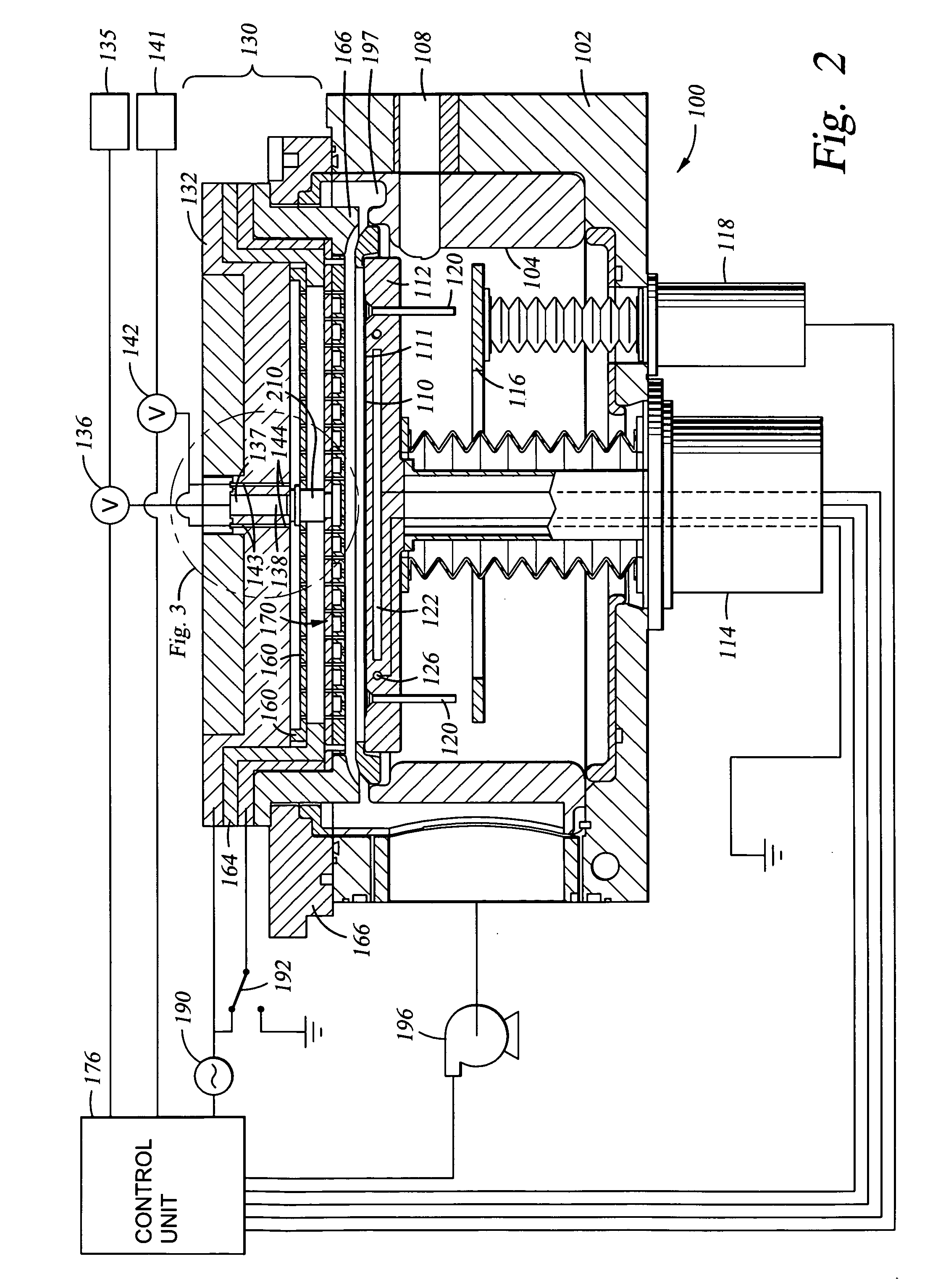
[0028]FIG. 2 is a schematic cross-sectional view of one embodiment of a chamber 100 adapted to generate a plasma within the gas distribution system of the processing chamber. The chamber 100 comprises a chamber body 102 having a liner 104 disposed therein. An opening 108 in the chamber 100 provides access for a robot (not shown) to deliver and retrieve substrates 110, such as, for example, 200 mm semiconductor wafer, 300 mm semiconductor wafers or glass substrates, to the chamber 100.

[0029] A substrate support 112 supports the substrate 110 on a substrate receiving surface 111 in the chamber 100. The substrate support 112 is mounted to a lift motor 114 to raise and lower the substrate support 112 and a substrate 110 disposed thereon. A lift plate 116 connected to a lift motor 118 is mounted in the chamber and raises and lowers pins 120 movably disposed through the substrate support 112. The pins 120 raise and lower the substrate 110 over the surface of the substra...


PUM

PropertyMeasurementUnit
thicknessaaaaaaaaaa
diameteraaaaaaaaaa
distanceaaaaaaaaaa

Abstract

Embodiments of the present invention relate to an apparatus and method of plasma assisted deposition by generation of a plasma adjacent a processing region. One embodiment of the apparatus comprises a substrate processing chamber including a top shower plate, a power source coupled to the top shower plate, a bottom shower plate, and an insulator disposed between the top shower plate and the bottom shower plate. In one aspect, the power source is adapted to selectively provide power to the top shower plate to generate a plasma from the gases between the top shower plate and the bottom shower plate. In another embodiment, a power source is coupled to the top shower plate and the bottom shower plate to generate a plasma between the bottom shower plate and the substrate support. One embodiment of the method comprises performing in a single chamber one or more of the processes including, but not limited to, cyclical layer deposition, combined cyclical layer deposition and plasma-enhanced chemical vapor deposition; plasma-enhanced chemical vapor deposition; and / or chemical vapor deposition.

Description

CROSS-REFERENCE TO RELATED APPLICATIONS [0001] This application claims benefit of U.S. patent application Ser. No. 10 / 197,940, filed Jul. 16, 2002 and U.S. Provisional Patent Application Ser. No. 60 / 352,191, filed Jan. 26, 2002, which are both herein incorporated by reference.BACKGROUND OF THE INVENTION [0002] 1. Field of the Invention [0003] Embodiments of the present invention generally relate to an apparatus and method for plasma assisted deposition. More particularly, embodiments of the present invention relate to an apparatus and method of plasma assisted deposition by generation of a plasma adjacent a processing region. [0004] 2. Description of the Related Art [0005] Reliably producing sub-micron and smaller features is one of the key technologies for the next generation of very large scale integration (VLSI) and ultra large scale integration (ULSI) of semiconductor devices. However, as the fringes of circuit technology are pressed, the shrinking dimensions of interconnects in...

Claims


Application Information

Patent Timeline
Patent Type & Authority Applications(United States)
IPC IPC(8): C23C16/00C23C16/06C23C16/34C23C16/42C23C16/44C23C16/452C23C16/455C23C16/515H01J37/32H01L21/285H01L21/312H01L21/768
CPCC23C16/06C23C16/34C23C16/42C23C16/452C23C16/4554C23C16/45544C23C16/45565C23C16/515H01J37/32082H01J37/3244H01L21/28556H01L21/28562H01L21/28568H01L21/3122H01L21/3127H01L21/76843H01L21/02216H01L21/0212
Inventor CHEN, CHEN-ANGELATOS, AVGERINOSYANG, MICHAEL X.XI, MINGHYTROS, MARK M.
Owner APPLIED MATERIALS INC
Why Eureka
Try Eureka