

Rectifier circuit
- Summary
- Abstract
- Description
- Claims
- Application Information
AI Technical Summary
Benefits of technology
Problems solved by technology
Method used
Image

Examples
first embodiment
[0035] the present invention will be described in detail below with reference to the accompanying drawings, wherein like reference numerals refer to like elements throughout.
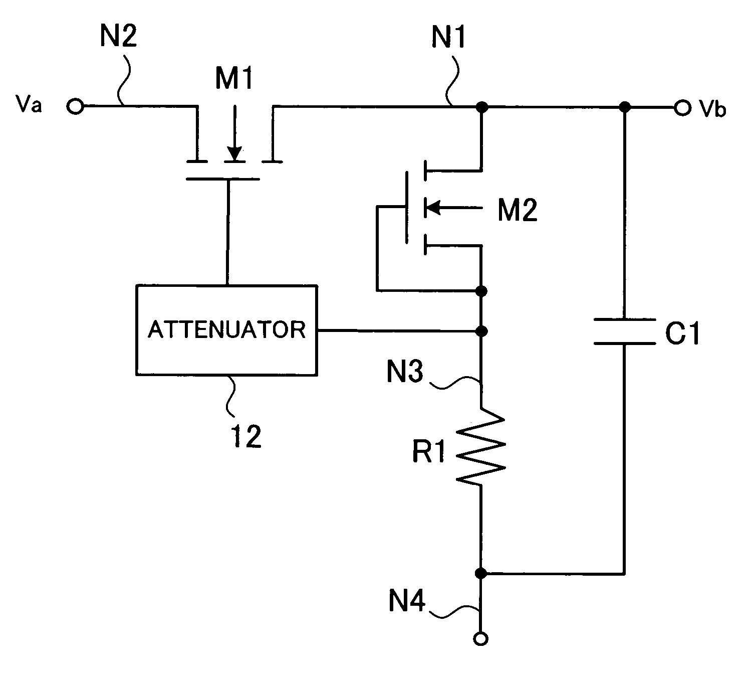
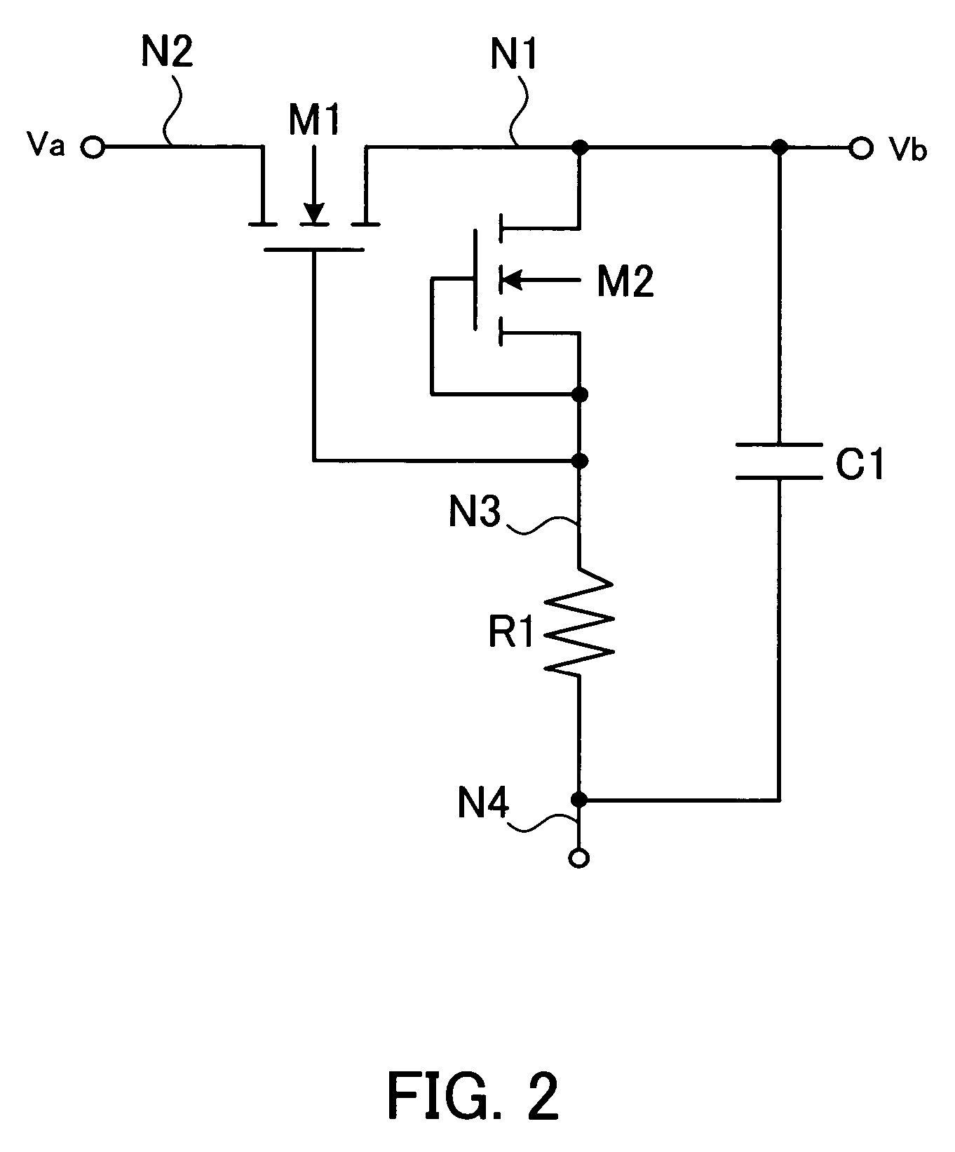
[0036]FIG. 1 is a circuit diagram of a rectifier circuit according to the first embodiment of the present invention. An NMOS transistor M1 shown in the diagram has a threshold voltage Vthn1. Nodes N1 and N2 serve as a drain and source of the transistor M1. A voltage Va to be rectified is inputted to the node N2 and a rectified voltage Vb is outputted to the node N1.
[0037] A threshold voltage generator 11 is connected to a gate of the transistor M1 and the node N1. The threshold voltage generator 11 generates a voltage Vth1 and outputs it to the gate of the transistor M1. The voltage Vth1 is a voltage which is elevated by the threshold voltage Vthn1 with respect to a voltage of the node N1 and is decreased by a voltage ΔVthn sufficiently small with respect to the threshold voltage Vthn1.
[0038] In this circuit, ...
second embodiment
[0067]FIG. 7 is a circuit diagram of a rectifier circuit according to the present invention. A PMOS transistor M11 shown in the diagram has a threshold voltage Vthp1. Nodes N11 and N12 each serve as a drain and source of the transistor M11. The voltage Va to be rectified is inputted to the node N12 and the rectified voltage Vb is outputted to the node N11.
[0068] The threshold voltage generator 21 is connected to the gate of the transistor M11 and the node N11. The threshold voltage generator 21 generates a voltage Vthh and outputs it to the gate of the transistor M11. The voltage Vthh is a voltage which is decreased by the threshold voltage Vthp1 with respect to a voltage of the node N11 and is elevated by a voltage ΔVthp sufficiently small with respect to the threshold voltage Vthp1.
[0069] In the circuit, when the voltage Va is higher than the voltage Vb, a positive charge flows from the node N12 to the node N11. Therefore, the node N12 serves as the source. Accordingly, when the ...
PUM
 Abstract
Description
Claims
Application Information