Methods relating to singulating semiconductor wafers and wafer scale assemblies

a technology of semiconductor wafers and scale assemblies, applied in the field of methods, can solve the problems of limited damage and thermal and achieve the effects of reducing the thickness of the wafer, less width, and limited damage potential of the resulting di

Active Publication Date: 2006-04-13
MICRON TECH INC
View PDF16 Cites 72 Cited by
  • Summary
  • Abstract
  • Description
  • Claims
  • Application Information

AI Technical Summary

Benefits of technology

[0013] The wafer is then singulated along the streets from the active surface side thereof with a laser beam, which may be of lesser width than the trenches. Potential damage to the resulting dice may be limited by using a narrower laser beam to cut through the reduced thickness of the wafer along the trenches, lessening the potential for thermal stress due to a reduction in the time and energy required for singulation and increasing the distance from the integrated circuitry on the active surface near the periphery of the semiconductor dice. The required width of the streets on the active surface of the wafer may thus be reduced, making additional wafer area available for semiconductor die fabrication.
[0014] In another embodiment, the present invention comprises providing additional edge protection at the perimeters of the active surfaces of the semiconductor dice by forming channels, or trenches, along the streets from the active surface of the wafer, filling the channels or trenches with a protective material such as a dielectric, and then singulating the semiconductor dice using a laser beam of lesser width than the trenches and directed along paths substantially centered within the trenches, leaving a coating of the protective material along sidewalls of the channels or trenches at the perimeters of the active surfaces of the semiconductor dice.

Problems solved by technology

Potential damage to the resulting dice may be limited by using a narrower laser beam to cut through the reduced thickness of the wafer along the trenches, lessening the potential for thermal stress due to a reduction in the time and energy required for singulation and increasing the distance from the integrated circuitry on the active surface near the periphery of the semiconductor dice.

Method used


Image

  • Methods relating to singulating semiconductor wafers and wafer scale assemblies
  • Methods relating to singulating semiconductor wafers and wafer scale assemblies
  • Methods relating to singulating semiconductor wafers and wafer scale assemblies

Examples


Embodiment Construction

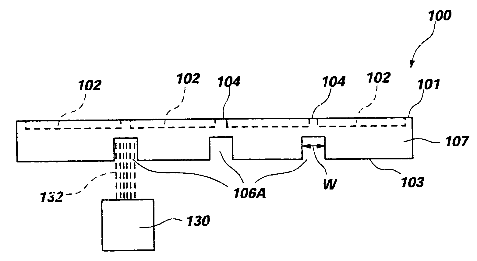
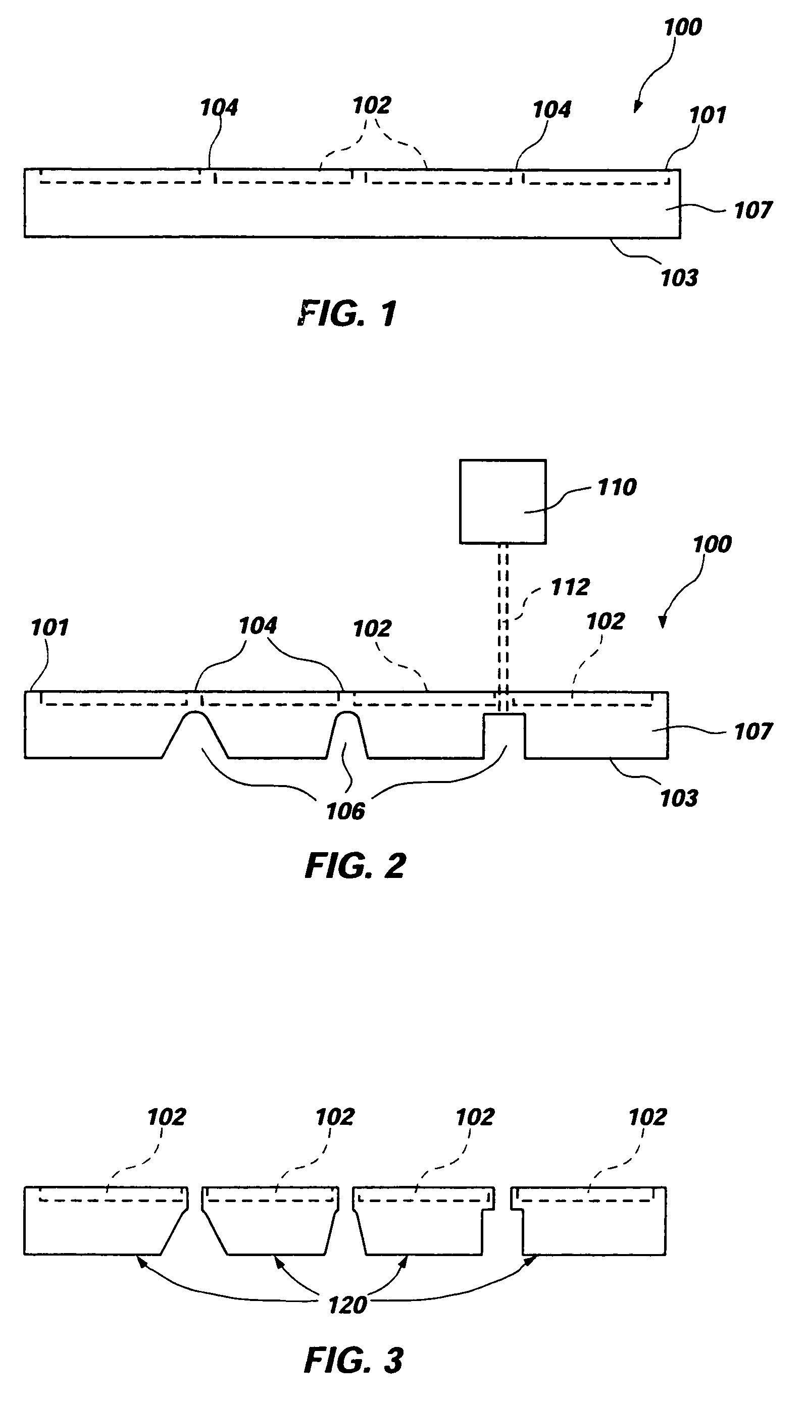
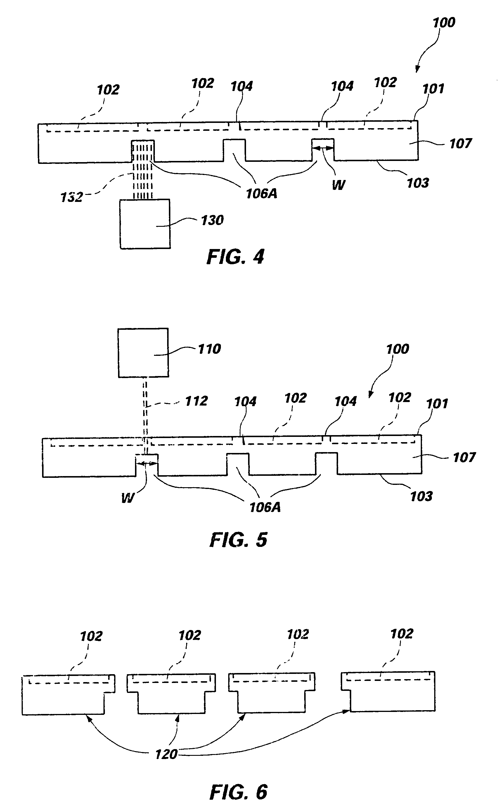
[0032] As used herein, the term “wafer” is not limited to conventional wafers of silicon or other semiconductor materials but also includes bulk substrates including a layer of semiconductor material carried by a supporting structure including, without limitation, silicon on insulator (SOI) substrates as exemplified by silicon on glass (SOG) and silicon on sapphire (SOS) substrates, as well as other structures known to those of ordinary skill in the art. Further, the terms “active surface” and “top surface” may be used interchangeably herein to designate a surface of a wafer having integrated circuitry fabricated thereon, while the terms “back side,” back surface,” and “bottom surface” may be used interchangeably herein to designate a surface of a wafer opposite that on which integrated circuitry is fabricated. Hence, the use of directional terminology is for convenience and to facilitate understanding of the present invention and the practice thereof, and not by way of limitation, ...


PUM

PropertyMeasurementUnit
thicknessaaaaaaaaaa
thicknessaaaaaaaaaa
temperatureaaaaaaaaaa

Abstract

Methods relating to the singulation of dice from semiconductor wafers. Trenches or channels are formed in the bottom surface of a semiconductor wafer, corresponding in location to the wafer streets. The trenches may be formed by etching or through an initial laser cut. The wafer is then singulated along the streets with a laser preferably having a beam narrower than the trenches. Multiple, laterally spaced lasers may be used in combination during a single pass to perform simultaneous singulating cuts. Additional edge protection for integrated circuitry on the active surface of the semiconductor dice may be provided by forming trenches or channels along the streets in the active surface instead of the bottom surface, disposing protective material along the streets and within the trenches prior to singulation and cutting through the wafer, leaving protective material on the sidewalls of the channels.

Description

CROSS-REFERENCE TO RELATED APPLICATION [0001] This application is a divisional of application Ser. No. 10 / 797,504, filed Mar. 10, 2004, pending.BACKGROUND OF THE INVENTION [0002] 1. Field of the Invention [0003] The present invention relates to methods and apparatus for cutting semiconductor wafers and wafer scale assemblies for singulation into dice or groups of die locations. More particularly, but not limited thereto, the present invention relates to the singulating of semiconductor wafers and wafer scale assemblies using laser cutting, alone or in combination with other techniques, to enable a reduction in the required width of streets between semiconductor die locations. [0004] 2. State of the Art [0005] Singulating semiconductor wafers, also known as dicing or die separation, is the process of cutting a semiconductor substrate having integrated circuits formed thereon into individual semiconductor dice. Currently, although a number of methods for singulating semiconductor wafe...

Claims


Application Information

Patent Timeline
Patent Type & Authority Applications(United States)
IPC IPC(8): H01L21/50H01L21/30H01L21/78H01L21/301H01L21/46
CPCB23K26/367B23K26/4075B28D1/221B28D5/00H01L21/78B23K26/364B23K26/40H01L2224/11B23K2103/50H01L2924/10156
Inventor AKRAM, SALMAN
Owner MICRON TECH INC
Why Eureka
Try Eureka