Desoldering wick for lead-free solder

Inactive Publication Date: 2006-04-20
HAKKO CO LTD
16 Cites 7 Cited by

AI-Extracted Technical Summary

Problems solved by technology

When using a desoldering tool with an electric vacuum pump, a problem may arise when solder remaining on the desoldering tip is left on the circuit board.
The residual solder must be removed by an additional cleaning step, and this step may jeopardize the integrity of the electronic circuit board.
However, a large amount of flux coated on the metal wires is associated with at least two problems.
Such activators are corrosive to electrical circuits, a typical substrate on which solder is used.
Thus, any residual flux remaining on the circuit board may have to be removed after desoldering, jeopardizing the integrity of the circuit board.
Additionally, exposure to flux is associated with various health problems.
Thus, use of this type of desoldering wick typically requires twice as long to melt lead-free solder.
The tin, however, tends to oxidize as heat is applied to the wick resulting in lesser absorption capabilities.
With the advent of lead-free solder being broadly used, problems have arisen when an electronic device requires a desoldering application, for example, to change out an electrical component.
One such problem is that, when compared to lead-based solders, the melting points of lead-free solders are higher.
Because higher temperatures must be used, the heat applied to the desoldering wic...

Method used

[0040] The second noble metal layer 106 of the desoldering wick 100 assists in faster absorption of the lead-free solder 200. Because a noble metal has the property of having extremely high wettability, a typical lead-free solder 200 with low wettability will be absorbed faster by contact with the second noble metal layer 106 of the desoldering wick 100. In conventional desoldering wicks, flux in an amount up to three weight percent of a desoldering wick is used to absorb solder faster. The following Table illustrates the high weight percent of flux included in conventional desoldering wicks: TABLESample Wick ASample Wick BSample Wick C123123123Weight before cleaning (mg)349.6357.4352.9361.8364.5368.2484.1481.1477.3Weight after cleaning (mg)346.3353.3348.9353.7357.8360468.5465.7462.3Difference(mg)3.34.148.16.78.215.615.415Flux contents (wt. %)0.9441.1471.1332.2391.8382.2273.2223.2013.143Number of copper threads11012096
[0041] Thus, as shown, conventional wick A includes flux in the amount of approximately >1.0 weight percent, conventional wick B includes flux in the amount of approximately >2.0 weight percent and conventional wick C includes flux in the amount of approximately >3.0 weight percent of a conventional desoldering wick, respectively. However, a large amount of flux applied to a desoldering wick has the limitations as described herein. Advantageously, the application of the second noble metal layer 106 on the desoldering wick 100 substantially reduces the need for flux to an amount approximately equal to 0.01 to 0.5 weight percent of the desoldering wick 100 while simultaneously maintaining high absorbability.
[0042] Moreover, due to inherent properties of noble metals, the second noble metal layer 106 is not as susceptible to oxidation as is, for example, tin without a coating. The second noble metal coating 106 therefore advantageousl...

Benefits of technology

[0013] In one embodiment of the desoldering wick of the present invention, the second noble metal layer may be used as a visual indicator to distinguish a used portion from an unused portion of the desoldering wick. In an embodiment wherein the noble metal layer is gold, the unused portion of the wick will appe...

Abstract

A desoldering wick having an inner metal coating such as a 0.1 μm to 12 μm layer of tin or tin-alloy and an outer noble metal coating such as a 0.5 nm to 10 μm layer of gold, silver, platinum, palladium, or rhodium for the removal of lead-free solder; a method of manufacturing the desoldering wick; and methods of using the wick.

Application Domain

Soldering apparatusMetal working apparatus +1

Technology Topic

Pt elementPalladium +8

Image

  • Desoldering wick for lead-free solder
  • Desoldering wick for lead-free solder
  • Desoldering wick for lead-free solder

Examples

  • Experimental program(1)

Example

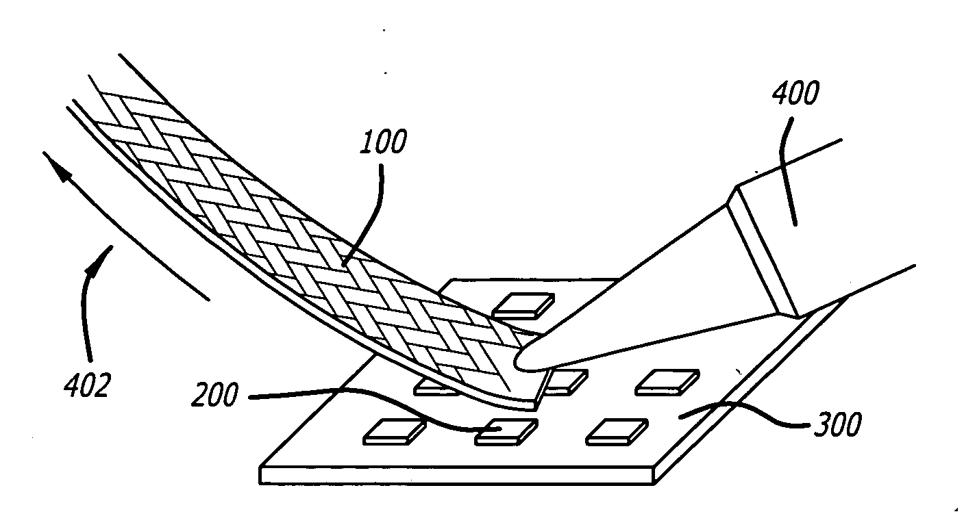
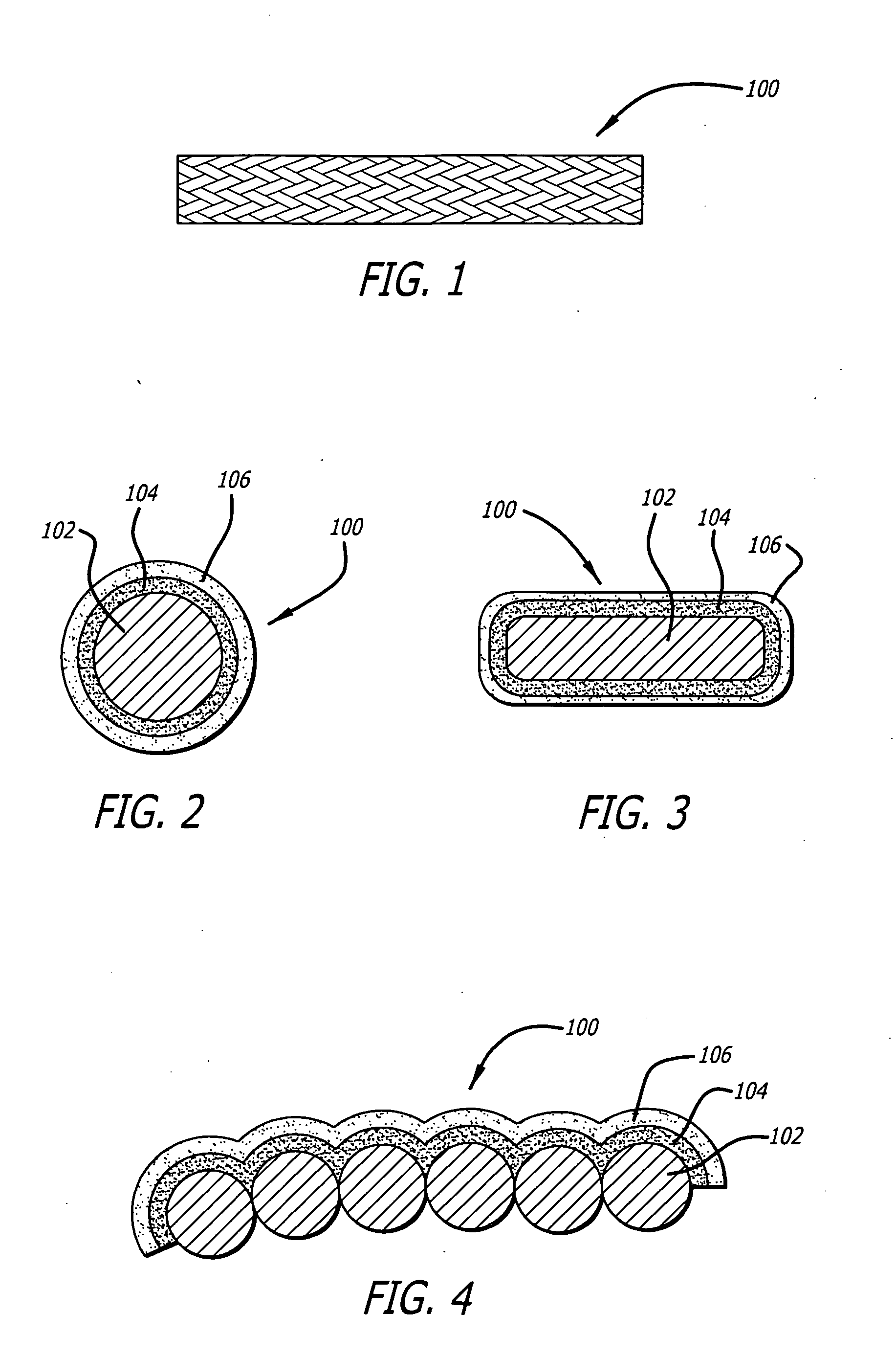
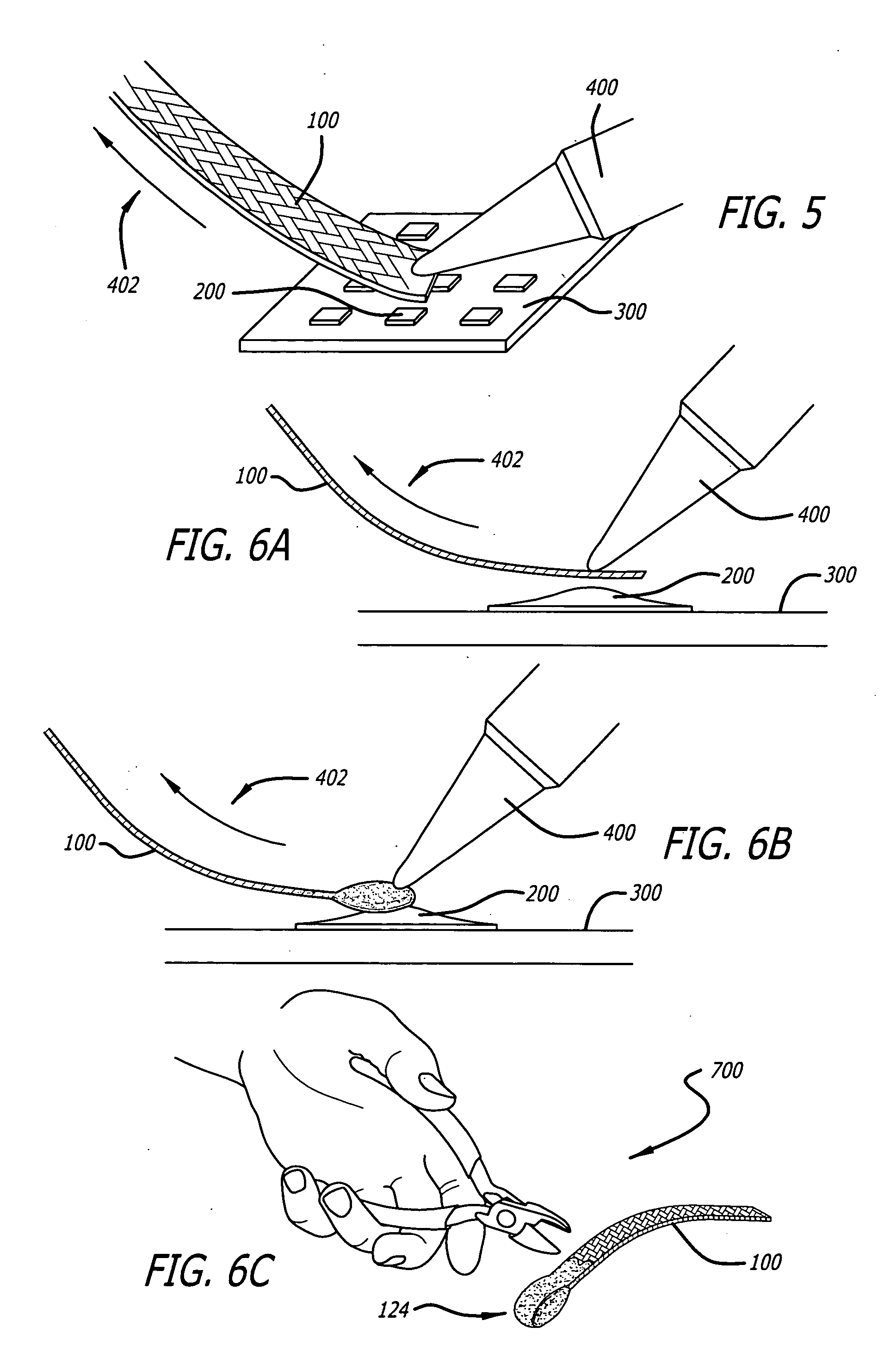
[0032] Referring to the drawings wherein like reference numerals designate like elements, FIG. 1 illustrates a preferred embodiment of a desoldering wick shown generally at 100 of the present invention. The desoldering wick 100 comprises a plurality of braided metal filaments 102 which are plated with a first metal coat 104 and a subsequent second noble metal coat 106. Between ninety and one hundred and twenty (and preferably one hundred and five) filaments are braided together to form the wick. The desoldering wick may be one to eight mm in width, typically four mm. Generally, the metal filaments 102 are comprised of copper, however, other suitable metals may be employed. Additionally, the metal filaments 102 are typically sixty μm to one hundred μm in diameter. The first metal coat 104 may be an elemental metal or a metal alloy. More specifically, the elemental metal of the first metal coat 104 may be, for example, tin, and the metal alloy of the first metal coat 104 may be a tin alloy, for example, tin-copper, tin-silver-copper, tin-silver or tin-zinc. The second noble metal coat 106 may be silver, gold, platinum, palladium or rhodium.
[0033] A cross-section of a metal filament 102 after plating is illustrated in FIG. 2. Referring thereto, the first metal coating 104 is typically 0.1 to twelve μm in thickness, and preferably 0.5 to two μm. The second noble metal coating 106 is typically 0.5 nm to ten μm in thickness, preferably gold, platinum, palladium or rhodium are 0.5 to one hundred and fifteen nm, and preferably silver is 0.5 to ten μm. Platings of the first metal coating 104 and of the second noble metal coating 106 are described more fully below.
[0034]FIG. 3 represents a cross-section of the desoldering wick 100 of FIG. 1. In this illustration, a plurality of metal filaments 102 is braided prior to the application of the first metal coating 104 and the subsequent second noble metal coating 106. FIG. 4 more clearly illustrates the coating of the desoldering wick 100 after braiding.
[0035] In FIG. 5, the use of the desoldering wick 100 to remove lead-free solder 200 from a substrate 300 is shown. Generally, a lead-free solder may be comprised of tin-copper, tin-silver-copper, tin-silver, or tin-zinc. As shown, the desoldering wick 100 is applied to lead-free solder 200, while a desoldering iron 400 is applied to the desoldering wick 100. Once the lead-free solder becomes molten, the lead-free solder 200 will absorb (shown by arrow 402) into the interstitial spaces of the desoldering wick 100. Depending on the composition of the lead-free solder 200, the lead-free solder will become molten at a certain temperature, such temperature typically in the range of one hundred and eighty to two hundred and twenty-seven degrees Celsius. In FIG. 6A, a side view of the use of the desoldering wick 100 to remove lead-free solder 200 from a substrate 300 is shown.
[0036] Generally, the melting temperature of the soldering material which distinguishes between a soldering work and a brazing work is 450 degrees Celsius. Lead-free solders for soldering work include tin-silver, tin silver copper, tin copper and tin zinc alloys. The melting temperatures of these materials (their liquidus temperatures) range from approximately 186 degrees Celsius to approximately 380 degrees Celsius. The first metal layer or coating 104 of the present wick 100 preferably should melt faster than the solder of the solid soldered joint so that the molten first metal on the wick will quickly transfer the heat from the soldering iron via the wick to the soldered joint (see FIGS. 5, 6A and 6B, for example). Therefore, a preferred melting temperature range of a low melting point metal (or alloy) herein is one having a melting temperature in the range of between 150 degrees Celsius to 350 degrees Celsius.
[0037] The following elementary metals are low melting point metals with melting points between 150 degrees Celsius and 350 degrees Celsius, and are listed below with their melting points in degrees Celsius: Indium (In), 156.2°; Lithium (Li), 180.5°; Tin (Sn), 232°; Polonium (Po), 254°; Bismuth (Bi), 274.1°; Thallium.(Ti), 303.5°; Cadmium (Cd), 320.8°; and Lead (Pb), 327°. The safest and least expensive of the above-listed elementary metals are indium, tin and bismuth.
[0038] Some lead-free solders contain copper, silver or antimony, which technically are not low melting point metals as their melting points are 1083°, 962° and 631° Celsius, respectively. Since these lead-free solders have the low melting point temperatures, they may be used as the low melting point metal (or alloy) of the first metal coat 104 of the desoldering wick 100. Tin is a preferred metal for the first metal or alloy coat 104 or layer, because tin is a common metal in all lead-free solders and tin residues on a joint do not materially change its composition. Additionally, tin has a melting point of 232° Celsius, which is approximately the midpoint in the above-mentioned temperature range of 150° to 350° Celsius for low melting point metals.
[0039] The first metal layer 104 of the desoldering wick 100 helps prevent heat from the desoldering iron 400 from flowing directly to the metal filaments 102 and, consequently, assists in directing the heat to the lead-free solder 200 itself. Thus, the lead-free solder 200 melts faster due to the first metal coating 104. The first metal layer 104 coating without a second oxidation-reducing coating, however, is susceptible to oxidation, rendering the removal of solder more difficult without the same.
[0040] The second noble metal layer 106 of the desoldering wick 100 assists in faster absorption of the lead-free solder 200. Because a noble metal has the property of having extremely high wettability, a typical lead-free solder 200 with low wettability will be absorbed faster by contact with the second noble metal layer 106 of the desoldering wick 100. In conventional desoldering wicks, flux in an amount up to three weight percent of a desoldering wick is used to absorb solder faster. The following Table illustrates the high weight percent of flux included in conventional desoldering wicks: TABLE Sample Wick A Sample Wick B Sample Wick C 1 2 3 1 2 3 1 2 3 Weight before cleaning (mg) 349.6 357.4 352.9 361.8 364.5 368.2 484.1 481.1 477.3 Weight after cleaning (mg) 346.3 353.3 348.9 353.7 357.8 360 468.5 465.7 462.3 Difference(mg) 3.3 4.1 4 8.1 6.7 8.2 15.6 15.4 15 Flux contents (wt. %) 0.944 1.147 1.133 2.239 1.838 2.227 3.222 3.201 3.143 Number of copper threads 110 120 96
[0041] Thus, as shown, conventional wick A includes flux in the amount of approximately >1.0 weight percent, conventional wick B includes flux in the amount of approximately >2.0 weight percent and conventional wick C includes flux in the amount of approximately >3.0 weight percent of a conventional desoldering wick, respectively. However, a large amount of flux applied to a desoldering wick has the limitations as described herein. Advantageously, the application of the second noble metal layer 106 on the desoldering wick 100 substantially reduces the need for flux to an amount approximately equal to 0.01 to 0.5 weight percent of the desoldering wick 100 while simultaneously maintaining high absorbability.
[0042] Moreover, due to inherent properties of noble metals, the second noble metal layer 106 is not as susceptible to oxidation as is, for example, tin without a coating. The second noble metal coating 106 therefore advantageously acts as an oxidation-reducing agent which further allows for easy removal of the lead-free solder.
[0043] In addition, the second noble metal layer 106 consisting of gold further may act as a visual indicator to distinguish unused portions from used portions of the desoldering wick 100, as shown in FIGS. 6A and 6B. After the desoldering wick 100 is used to remove lead-free solder from a substrate 300, the used portion 124 of the desoldering wick 100 will take on the color of the absorbed solder, typically gray. Thus, because the unused portion is gold in color, the unused portion is easily distinguished from the used portion 124. This reduces the risk of a user re-using a used portion 124 of the desoldering wick 100, which use may compromise the integrity of the substrate 300. Once the used portion 124 is distinguished from the unused portion, the used portion may be removed by a nipper or diagonal cutter 700, for example.
[0044] An alternative preferred embodiment of the desoldering wick 100 of the present invention is shown in FIG. 7. In this embodiment, the desoldering wick 100 is divided into small units and may be applied to a substrate 300 for removal of solder by using, for example, tweezers 500. This embodiment may be useful for removing lead-free solder 200 from very small electronic parts.
[0045]FIG. 8 is a bar graph shown generally at 600 comparing the melting rates of lead-free solder 200 using various desoldering wicks comprising at least a plurality of braided copper wires, and including a representative desoldering wick 100 of the present invention. The x-axis of the graph shows the time required for lead-free solder to start melting in seconds. The y-axis depicts various embodiments of a desoldering wick, each represented by a different bar. Shown on the y-axis, from left to right, are a desoldering wick with: tin plating at 1 μm, tin plating at 5 μm, tin plating at 10 μm, tin plating at 5 μm+gold plating at 5 nm, gold plating at 5 nm, copper with no plating and copper with no plating +flux, respectively. As shown, the melting rate of the lead-free solder 200 with application of the tin plating at 5 μm+gold plating at 5 nm, a preferred embodiment of the desoldering wick 100, is shown to be substantially the same as those coated with tin only in the amounts of 1 μm, 5 μm and 10 μm. Although a desoldering wick with tin in the amounts described may have a tendency to melt lead-free solder 200 slightly faster than the preferred embodiment, the tin of such desoldering wicks is susceptible to oxidation and thus less absorption capability as previously described. Also noteworthy is that desoldering wicks with 5 μm of gold only, no plating, and no plating+flux, respectively, all tend to melt solder at a substantially slower rate than that of the preferred embodiment. Accordingly, application of the desoldering wick 100 of the present invention advantageously results in a shorter amount of time needed to melt lead-free solder without compromising resistance to oxidation when compared to those desoldering wicks as illustrated in FIG. 8.
[0046]FIG. 9 represents a manufacturing process of the desoldering wick 100 of the present invention. The manufacturing process may be explained in a series of steps. First, a plurality of metal filaments 102 is braided into a barrel form 108. The barrel form 108 is then shaped to a flat form 110, or a braided wick, with a roller. Next, the braided wick is degreased, rinsed and activated. The degreasing solvent may be, for example, a combination of sodium hydroxide, a sodium silicate oxide and an activator, while the rinsing liquid may be water, and the activation solvent may be a 10% solution of hydrochloric acid. After activation, the braided wick is placed on a hangar-like device 114 in preparation for plating.
[0047] At least two plating baths 116a and 116b are provided for the plating process: one for application of the first metal coating 104 and another for the application of the second noble metal coating 106. The braided wick is plated with a first metal coating 104 in plating bath 116a, and then a second noble metal coating 106 in plating bath 116b. In an alternative embodiment, the twice-coated braided wick may be coated with a flux, such as rosin, by methods known in the art. The method of plating may be, for example, electroplating, chemical or electroless plating, all of which are well known methods of plating.
[0048] The thickness of the coating can be controlled by time and electrical current. For example, the first metal coating 104 may be applied by the immersion of the braided wick in a plating bath 116a for a period of between twelve seconds and twenty minutes, preferably approximately ten seconds, and subjected to between 0.2 to 2.0 amperes/dm2 of electrical current. Similarly, the second noble metal coating 106 may be applied by the immersion of the coated braided wick in a plating bath 116b for a period of between ten seconds and twenty minutes, preferably approximately thirty-five seconds, and subjected to between 0.2 to 2.0 amperes/dm2 of electrical current. The resulting twice-coated braided wick is then dried and ready for use (or a subsequent process step).
[0049]FIG. 10 shows an alternative manufacturing process of the desoldering wick 100. In this process, the metal filaments 102 undergo electroplating, chemical or electroless plating before braiding. Generally, the process is the same as that described in FIG. 9 except that the variables to control thickness,. such as time and electrical current, may need to be adjusted accordingly. For example, the first metal coating 104 may be applied by the immersion of the metal filament 102 in a plating bath 116a for a period of between twelve seconds and twenty minutes, preferably approximately ten seconds, and subjected to between 0.2 to 2.0 amperes/dm2 of electrical current. Similarly, the second noble metal coating 106 may be applied by the immersion of the coated metal filament 102 in a plating bath 116b for a period of between ten seconds and twenty minutes, preferably approximately thirty-five seconds, and subjected to between 0.2 to 2.0 amperes/dm2 amperes of electrical current. In an alternative embodiment, the twice-coated metal filament 102 may be coated with a flux, such as rosin, by methods known in the art. The resultant coated metal filaments 102 may then be braided into a barrel form 108 and subsequently shaped into a flat form by a roller. The resultant desoldering wick 100 may then be spooled on a bobbin 118 (see FIG. 11) and stored in a case 120 (see FIG. 12).
[0050] In FIG. 13, a cross-section of a metal filament 102 of an alternative embodiment of the desoldering wick 100 is shown. In this embodiment, the metal filament 102 is coated with a first metal coating 104, a second noble metal coating 106 and a third flux coating 122. The first metal coating 104 is typically 0.1 to 10 μm in thickness, preferably 0.5 to 2 μm. The second noble metal coating 106 is typically 0.5 to one hundred and fifteen nm thick, preferably gold, platinum, palladium, or rhodium is five to twenty nm, and preferably silver is 0.5 to ten μm. The third flux coating 122 is typically 0.01 to 0.5 weight percent of the desoldering wick 100.
[0051]FIG. 14 is a cross-section of an alternative embodiment of the desoldering wick 100 of FIG. 1. In this illustration, a plurality of metal filaments 102 is braided prior to the application of the first metal coating 104, the second noble metal coating 106 and the third flux coating 122. FIG. 15 more clearly illustrates the coating of the alternative embodiment of the desoldering wick 100 after braiding.
[0052] From the foregoing detailed description, it will be evident that there are a number of changes, adaptations and modifications of the present invention which come within the province of those skilled in the art. The scope of the invention includes any combination of the elements from the different species or embodiments disclosed herein, as well as subassemblies, assemblies, and methods thereof. However, it is intended that all such variations not departing from the spirit of the invention be considered as within the scope thereof.

PUM

PropertyMeasurementUnit
Length1.0E-7m
Length1.2E-5m
Length1.0E-5m

Description & Claims & Application Information

We can also present the details of the Description, Claims and Application information to help users get a comprehensive understanding of the technical details of the patent, such as background art, summary of invention, brief description of drawings, description of embodiments, and other original content. On the other hand, users can also determine the specific scope of protection of the technology through the list of claims; as well as understand the changes in the life cycle of the technology with the presentation of the patent timeline. Login to view more.

Similar technology patents

Ripcord of optic cables and method of manufacturing the same

InactiveUS20100129655A1easily distinguishexcellent mechanical property
Owner:KOLON IND INC

Audio matching

ActiveUS20210224318A1easily distinguish
Owner:INTRASONICS S A R L

Method for providing map information and electronic device for supporting the same

ActiveUS20200033154A1easily distinguish
Owner:SAMSUNG ELECTRONICS CO LTD

Water-containing lipstick and preparation method therefor

InactiveUS20210299015A1easily distinguishhigh water level
Owner:GLOBAL COSMETICS HONG KONG CO LTD

Analysis apparatus and method

InactiveUS20110244590A1easily distinguish
Owner:FUJIFILM CORP

Classification and recommendation of technical efficacy words

  • easily distinguish

Scroll Display Program, Device, and Method, and Electronic Device Provided with Scroll Display Device

ActiveUS20110099509A1easily distinguish
Owner:SONY COMPUTER ENTERTAINMENT INC

Display apparatus and control method thereof

InactiveUS20170038897A1easily distinguisheasily determine
Owner:SAMSUNG ELECTRONICS CO LTD

Wearable terminal device and image processing method

ActiveUS20170115752A1easily distinguish
Owner:SEIKO EPSON CORP
Why Eureka
Try Eureka