Fine pitch grid array type semiconductor device

a semiconductor device and grid array technology, applied in the field of semiconductor devices, can solve the problems of increasing pads, reducing the size not revealing the reduction in size (size shrinkage) of semiconductor chips used in semiconductor devices, etc., to achieve sufficient electrical characteristics, reduce the inductance of power supply, and reduce the size of chips

Active Publication Date: 2006-04-20
LONGITUDE LICENSING LTD
View PDF4 Cites 6 Cited by
  • Summary
  • Abstract
  • Description
  • Claims
  • Application Information

AI Technical Summary

Benefits of technology

[0012] The inventors have achieved a technique to solve the above-mentioned problems as the result of researches of techniques for achieving a reduction in size of chips while attaining sufficient electrical characteristics, namely, attaining lowered inductance in power supply and ground wires so as to reduce noise.

Problems solved by technology

However, although Patent Document 1 discloses an effective technique for reducing the power supply based inductance in the semiconductor device, Patent Document 1 does not disclose a reduction in size (size shrink) of a semiconductor chip used in the semiconductor device.
The connection technique in the post-process has not advanced rapidly as compared with the processing technique inside the chip.
Therefore, even if the size inside the chip is significantly reduced, there is a possibility in that connection is performed by only current pad sizes and current pad pitches under constraints on the connection means for the semiconductor chip and the package.
However, this causes an increase of pads to provide a problem of preventing a reduction in size of the semiconductor chip.
On the other hand, when attentions are paid to only size reduction of the semiconductor chip and then the number of power supply pads and ground pads is reduced excessively, it is impossible to make electrical characteristics, namely, inductance of power supply and ground wires small sufficiently, and, as a consequence, there is a problem in that the semiconductor device cannot be operated at high speed.
This situation causes a problem in that a further reduction in size of chip cannot be attained under constraints on pads to be arranged on the main surface of the chip regardless of the situation in that a reduction in size of the semiconductor chip can be attained by improvement of the production process for the semiconductor chip.

Method used


Image

  • Fine pitch grid array type semiconductor device
  • Fine pitch grid array type semiconductor device
  • Fine pitch grid array type semiconductor device

Examples


first embodiment

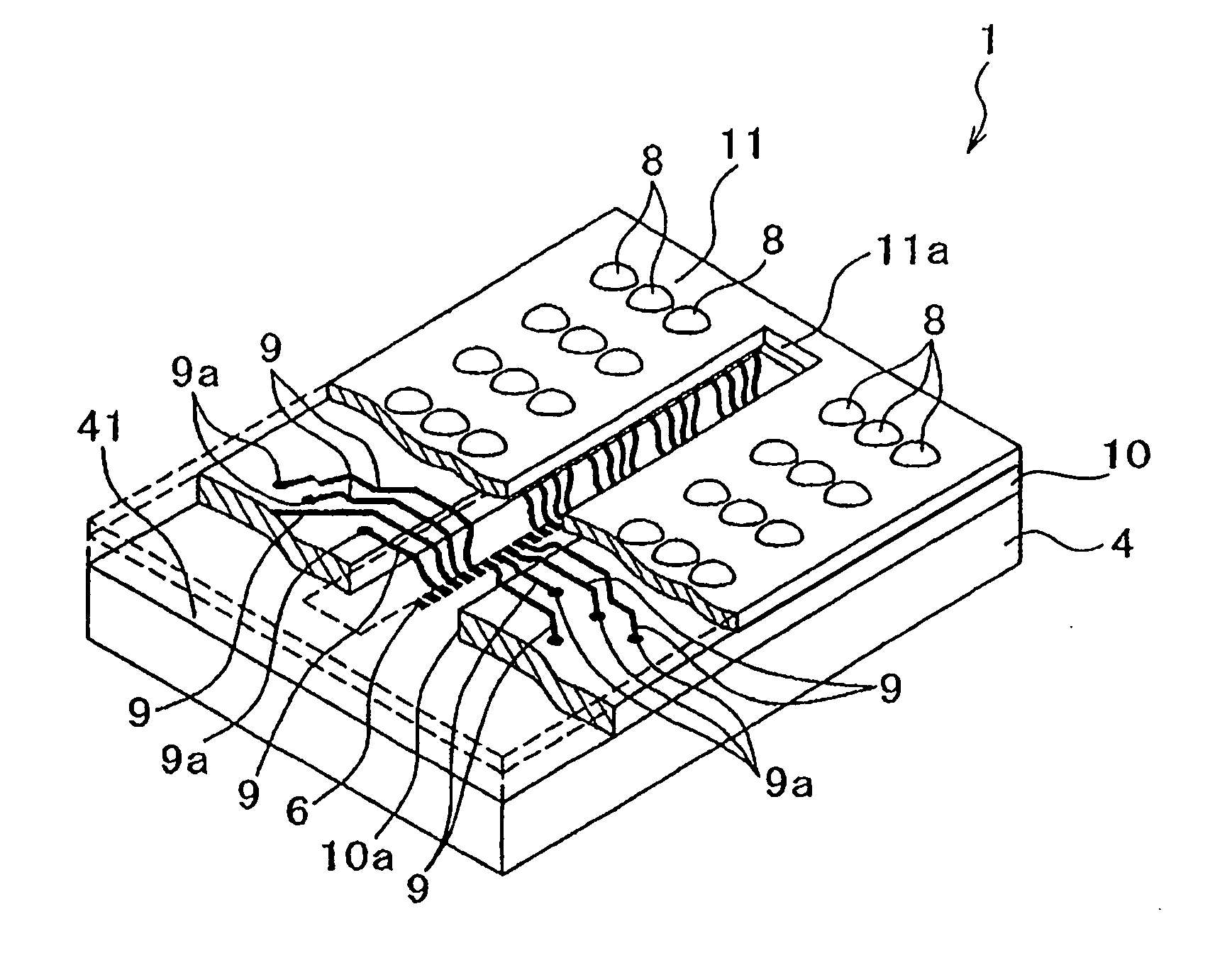
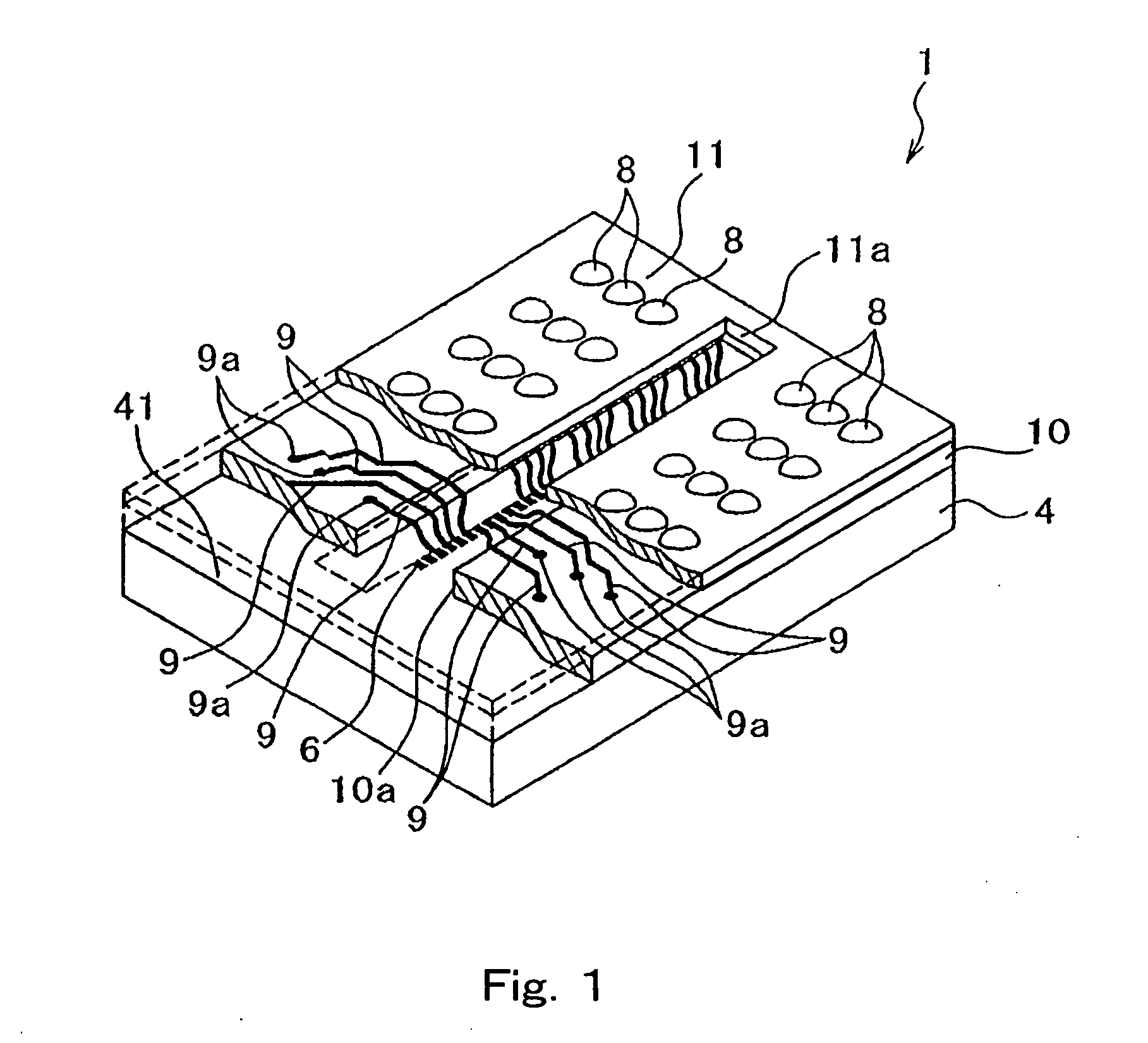
[0030] Referring to FIG. 1, semiconductor device 1 of the first embodiment according to the present invention is shown that includes semiconductor chip 4 and tape substrate 11 joined to semiconductor chip 4 via adhesive layer 10. Semiconductor chip 4 has a plurality of buffers 4a (refer to FIG. 2) to be DRAM components and a plurality of pads 6 arranged in the center on main surface 41 of semiconductor chip 4. Main surface 41 of semiconductor chip 4 is oriented to tape substrate 11. Tape substrate 11 is provided with a plurality of solder balls 8 to be external connection contacts. Solder balls 8 are arranged in grids. Pad 6 and solder ball 8 are electrically connected via wire 9.

[0031] Semiconductor device 1 is one example of a FBGA type DRAM, and pad 6 and solder ball 8 in semiconductor chip 4 are connected via wire 9 without a wiring board using wires and epoxy resin impregnated with glass. Tape substrate 11 is adhered to main surface 41 of semiconductor chip 4 via adhesive layer...

second embodiment

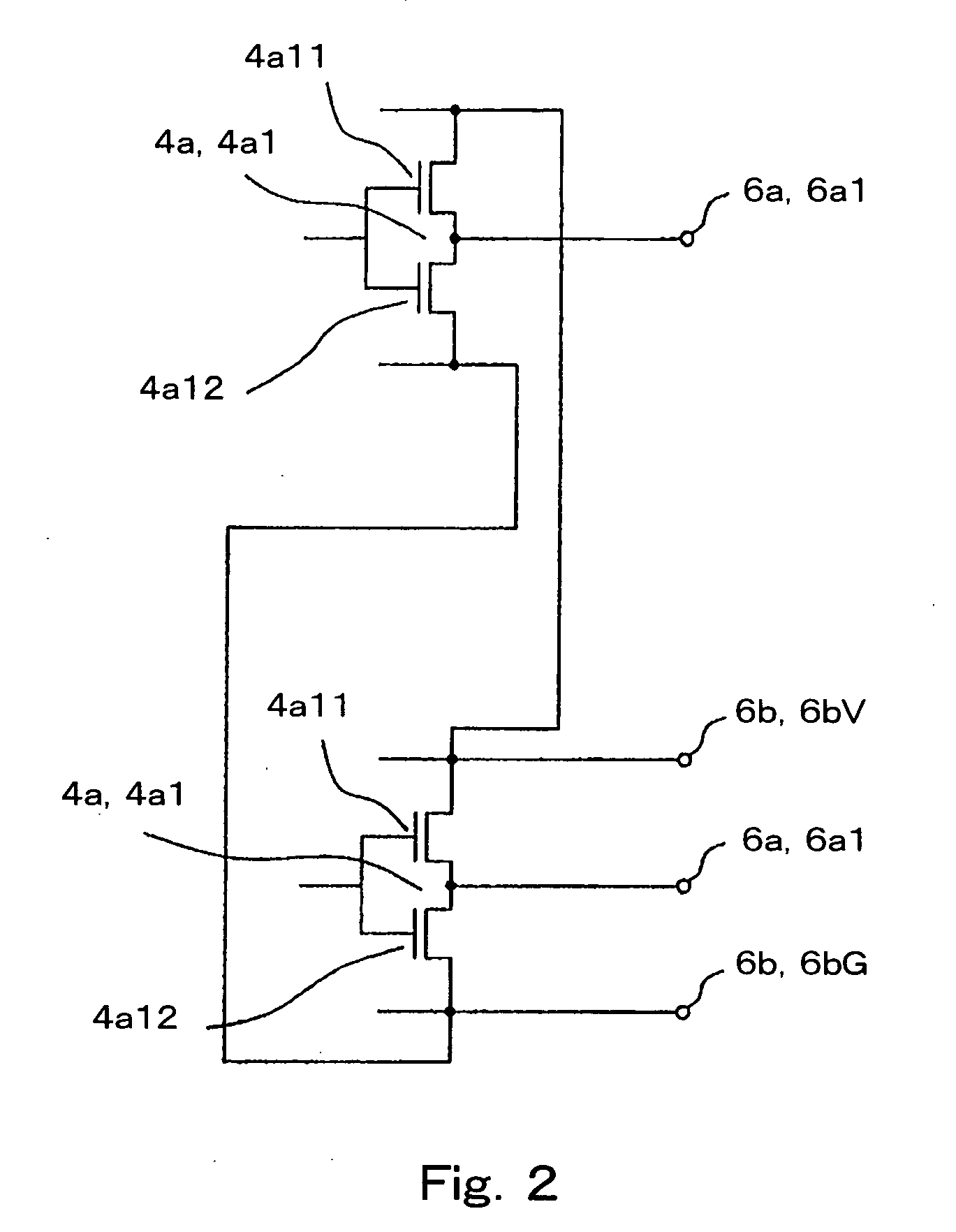
[0061] In the second embodiment, signal pads 6a2 are arranged at the outmost side in pad group 6A, power supply pad 6cV and ground pad 6cG connected with protection diodes 4b are arranged adjacently thereto at the inside, and power supply pad 6bV connected to the power supply and ground pad 6bG connected to the ground in input buffer 4a2 are arranged at the inside thereof.

[0062] When a total number of power supply pad 6cV and ground pad 6cG connected with protection diodes 4b and power supply pad 6bV connected to the power supply and ground pad 6bG connected to the ground in input buffer 4a2 is represented by N3, there is a relationship of N3 / (A / p)>0.3 between a total number (A / p) of pads which can be arranged in area A2 where pads can be arranged and the total N3. In this way, by ensuring power supply pad and ground pad which are important in high-speed operation, a reduction in noise, namely, high-speed operation can be attained. Further, there is no possibility that power supply ...

third embodiment

[0069] In the third embodiment, in order to compensate for weak points in power supply / ground series in input pad arrangement area 60c, a pair of power supply pad 61 and ground pad 62 is arranged at an approximate center of a line of pads in input pad arrangement area 60c as shown in FIG. 8. With this arrangement, electrical characteristics can be dramatically improved. In this case, when power supply pad 61 and ground pad 62 are respectively connected to the power supply and the ground connected to protection diodes associated with input pads, the best result can be obtained.

[0070] In FIG. 8, a wire is drawn from added power supply pad 61 to a solder ball for the power supply, and a wire is drawn from added ground pad 62 to a solder ball for the ground. As shown in FIG. 8, since a pair of wires for the power supply and the ground are drawn in mutually opposite directions while the center line of pads is regarded as an axis, outstanding effects on a reduction in noise can be obtaine...


PUM


Abstract

A semiconductor device has a semiconductor chip in which a plurality of semiconductor components and a plurality of pads are arranged, a plurality of external connection contacts arranged in grids, and a plurality of wires for electrically connecting the pads and the external connection contacts. The pads include a plurality of pad groups including a pair of electrode pads connected to the plurality of semiconductor components in common and a plurality of signal pads respectively connected to the semiconductor components connected to the electrode pads. In each pad group, each signal pad is arranged adjacently to one of the electrode pads; and each wire extending from each signal pad is extended along a wire extended from the electrode pad adjacent to each signal pad.

Description

BACKGROUND OF THE INVENTION [0001] 1. Field of the Invention [0002] The present invention relates to a semiconductor device, and more particularly to a semiconductor device preferably applied to a FBGA (Fine pitch Ball Grid Array) type DRAM (Dynamic Random Access Memory). [0003] 2. Description of the Related Art [0004] There is known a conventional semiconductor device disclosed in Japanese Patent Laid-Open No. 2001-185576 (Patent Document 1). The semiconductor device disclosed in Patent Document 1 is provided with pads for signal lines (signal pads), pads for a power supply potential (power supply pads), and pads for a ground potential (ground pads). In this semiconductor device, in order to reduce a power supply based inductance in the semiconductor device, all of the pads are formed on a surface of a wiring board, the surface connected with a semiconductor pellet (semiconductor chip) by wire bonding, and are connected with a signal contact, a power supply potential contact, and a...

Claims


Application Information

Patent Timeline
Patent Type & Authority Applications(United States)
IPC IPC(8): H01L23/48
CPCH01L23/49838H01L23/50H01L2924/15173H01L2924/15311H01L2924/3011H01L2924/30107H01L2924/13091H01L2224/4824H01L2924/00
Inventor KATAGIRI, MITSUAKISHIMIZU, HIROYAOSANAI, FUMIYUKITAKAHASHI, YASUSHINARUI, SEIJI
Owner LONGITUDE LICENSING LTD
Why Eureka
Try Eureka