Display device and method of manufacturing the same

a technology of display devices and manufacturing methods, applied in the direction of instruments, computing, electric digital data processing, etc., can solve the problems of user glare, change the maximum luminance required for the display device, and inability to control luminan

Inactive Publication Date: 2006-04-20
SEMICON ENERGY LAB CO LTD
View PDF17 Cites 63 Cited by
  • Summary
  • Abstract
  • Description
  • Claims
  • Application Information

AI Technical Summary

Benefits of technology

[0012] In order to solve the above problems, an object of the present invention is therefore to realize a display device in which the luminance can be automatically controlled in response to the brightness of the surrounding, and the luminance can be suitably controlled in accordance with a change in the brightness of the surrounding that the human senses.

Problems solved by technology

However, in many conventional display devices, an input voltage characteristic for image display is fixed, and thus sufficient attention is not paid such that a maximum luminance required for the display device is changed in response to a surrounding.
However, in this case, the luminance is not controlled.
Thus, a user will see a glare and visibility is deteriorated in many cases.
However, when those sensors are mounted as separate parts on the display device, a further area is required for the sensors.
As a result, there is a problem that a difference is produced between the brightness of the surrounding and the luminance correction.
Also, there is a problem that, although dependent on a kind of sensor, if an optical filter is not attached to the display device in order to fit a spectral sensitive characteristic of a sensor to a luminosity of a person, an error in the correction is produced.
Therefore, an enlargement of the display device cannot be prevented.

Method used


Image

  • Display device and method of manufacturing the same
  • Display device and method of manufacturing the same
  • Display device and method of manufacturing the same

Examples


embodiment 1

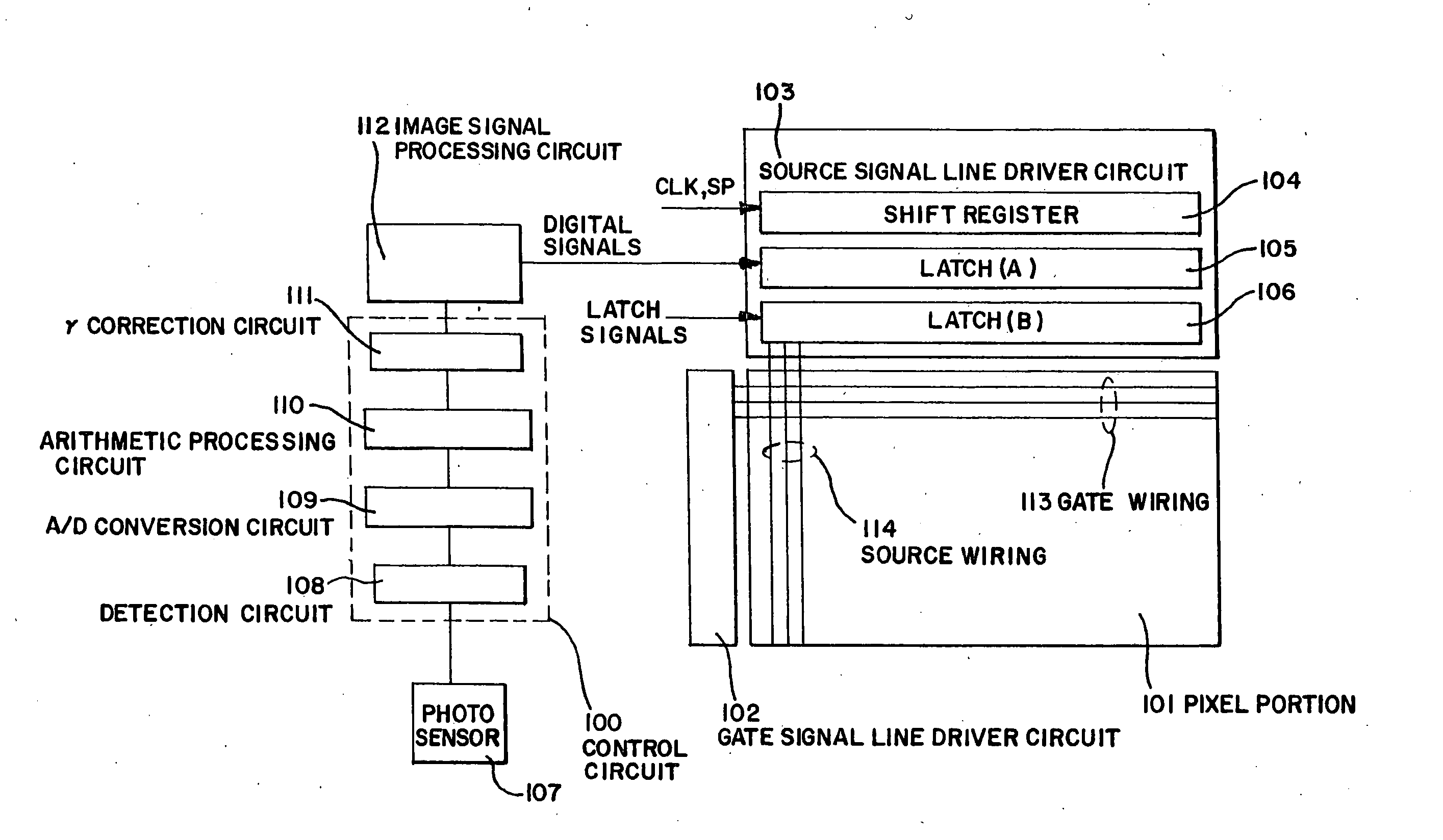
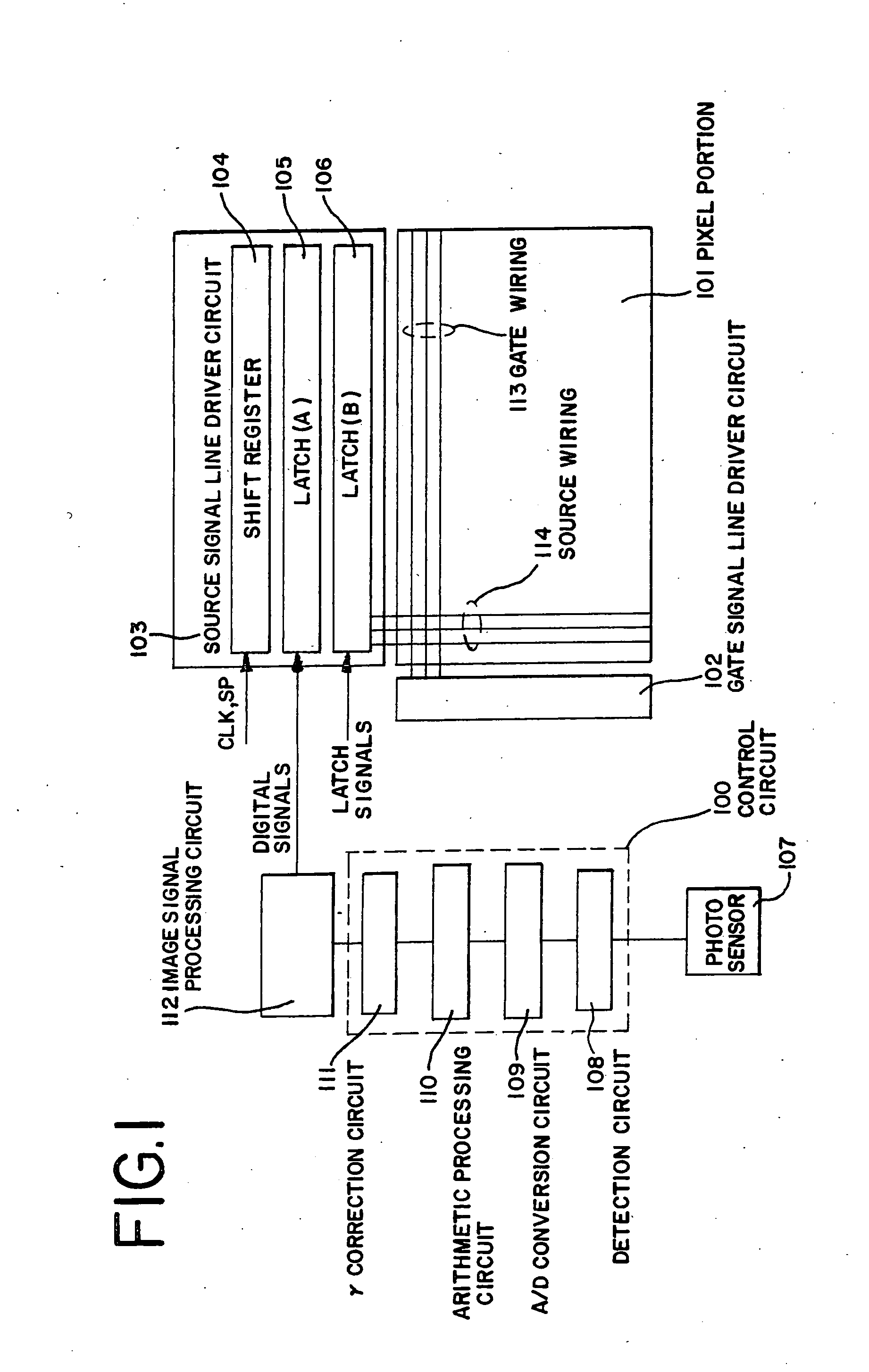
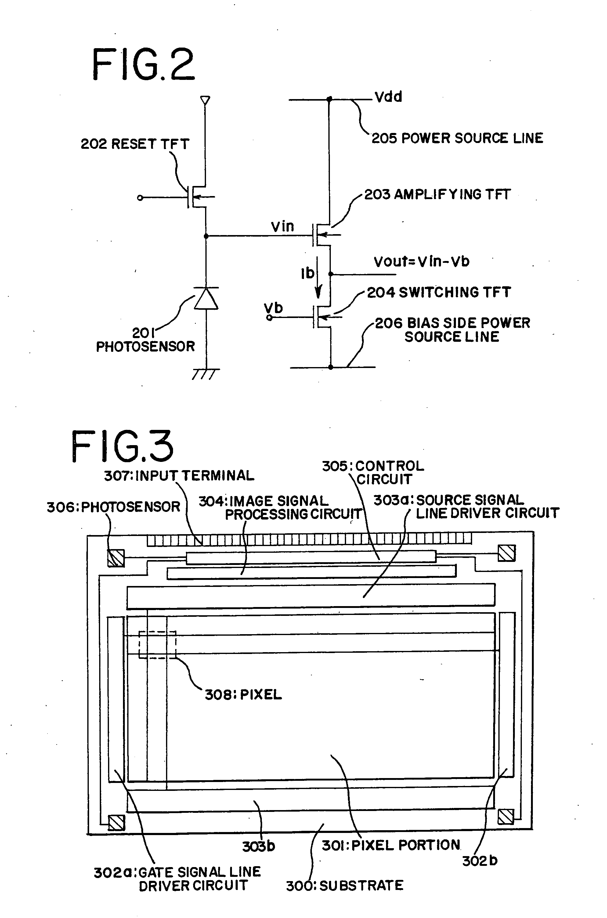
[0060]FIG. 3 is a schematic view of an active matrix display device having an automatic luminance control function. A pixel portion 301, gate signal line driver circuits 302a and 302b, source signal line driver circuits 303a and 303b, a control circuit 305, an image signal processing circuit 304, input terminals 307, and photosensors 306 are provided on a substrate 300 having an insulating surface. As shown in FIG. 3, the plurality of photosensors 306 are provided in outer portions of the substrate 300. When the plurality of photosensors 306 are provided, lights with various angles are detected, and thus the luminance can be delicately controlled.

[0061] The photosensors 306 are manufactured using a material such as amorphous silicon having a photoelectric effect. The photosensors 306 are manufactured on another substrate and then attached onto the outer portions of the substrate 300 outside the pixel portion 301 and the driver circuits on the substrate 300. In this case, light rece...

embodiment 2

[0066] The active matrix display device shown in FIG. 3 can be realized the liquid crystal display device and the EL display device. In this embodiment, the example of forming the TFT on the substrate and manufacturing the liquid crystal display device is explained.

[0067] First, as shown in FIG. 4A, a blocking layer 402 is formed of an insulating film such as a silicon oxide film, a silicon nitride film, or a silicon oxynitride film on a glass substrate 401 made of barium borosilicate glass represented by such as #7059 glass or #1737 glass of Corning Inc., or alumino borosilicate glass. For example, a silicon oxynitride film with a thickness of 10 to 200 nm (preferably 50 to 100 nm) is manufactured by a plasma CVD method from SiH4, NH3, and N2O, and a silicon hydride oxynitride film manufactured similarly from SiH4 and N2O is laminated and formed with a thickness of 50 to 200 nm (preferably 100 to 150 nm). In this embodiment, the blocking layer 402 is shown as a two layer structure...

embodiment 3

[0091]FIG. 16 shows one example of an active matrix display device manufactured using inverse stagger type TFTs. As Embodiment 2, a peripheral circuit 1705 formed by a p-channel TFT 1701 and an n-channel TFT 1702 and a pixel portion 1706 having a pixel TFT 1703 and a storage capacitor 1704 are formed on a substrate 1601. In FIG. 16, only cross sectional views of the p-channel TFT 1701 and the n-channel TFT 1702 in the peripheral circuit 1705 are shown. However, the gate signal line driver circuit, the source signal line driver circuit, the image signal processing circuit, and the control circuit, as described in Embodiment 1, can be formed using these TFTs.

[0092] Gate electrodes 1602 to 1604, source and drain lines 1606 and 1607, and a capacitor wiring 1605 are formed on the substrate 1601 by using a material selected from molybdenum (Mo), tungsten (W), tantalum (Ta), aluminum (Al), and the like. Then, a first insulating film 1608 which is an insulating film containing silicon and ...


PUM


Abstract

There is provided a display device capable of automatically controlling a luminance in response to a brightness of a surrounding. The display device has a gamma correction circuit for converting an image signal voltage into a drive voltage for gray scale display and a photosensor for controlling an input and output voltage characteristic of the gamma correction circuit in response to the brightness of the surrounding. In this case, the gamma correction circuit for converting the image signal voltage into the driver voltage for gray scale display is formed on a first substrate. The photosensor for controlling the input and output voltage characteristic of the gamma correction circuit in response to the brightness of the surrounding is formed on a second substrate. The second substrate is fixed to the first substrate.

Description

BACKGROUND OF THE INVENTION [0001] 1. Field of the Invention [0002] The present invention relates to a display device in which the luminance of a display screen can be controlled in response to the brightness of a surrounding and a method of manufacturing the same. [0003] 2. Description of the Related Art [0004] A technique for forming a thin film transistor (hereinafter referred to as a TFT) on a substrate is greatly improved, and thus the application to an active matrix display device is progressing. Conventionally, the active matrix display device utilized by TFTs using an amorphous silicon film requires a driver IC. However, TFTs using a polycrystalline silicon film can be operated with a high driver frequency, and TFTs in a pixel portion and TFTs in a driver circuit can be integrally formed on a substrate. [0005] The active matrix display device in which the driver circuit is integrally formed on the substrate has gathered attention, because various advantages such as a cost re...

Claims


Application Information

Patent Timeline
Patent Type & Authority Applications(United States)
IPC IPC(8): G09G5/00G09G3/20G09G3/30G09G3/32G09G3/36
CPCG09G3/2018G09G3/2022G09G3/30G09G3/3233G09G3/3648G09G2300/0426G09G2300/0842G09G2320/0276G09G2320/043G09G2320/0626G09G2360/144
Inventor YAMAZAKI, SHUNPEIARAI, YASUYUKIKIMURA, HAJIME
Owner SEMICON ENERGY LAB CO LTD
Why Eureka
Try Eureka