Memory device

Active Publication Date: 2006-04-20
MICRON TECH INC
View PDF17 Cites 28 Cited by
  • Summary
  • Abstract
  • Description
  • Claims
  • Application Information

AI Technical Summary

Benefits of technology

[0009] In view of the state of the art outlined in the foregoing, the Applicant has faced the problem of

Problems solved by technology

The unavoidable capacitive coupling between selected bit lines (accessed bit lines) and bit lines adjacent thereto (side bit lines) causes the generation of a current noise signal on the selected bit lines.
This problem of bit line capacitive coupling, also referred to a

Method used


Image

  • Memory device
  • Memory device
  • Memory device

Examples


Example

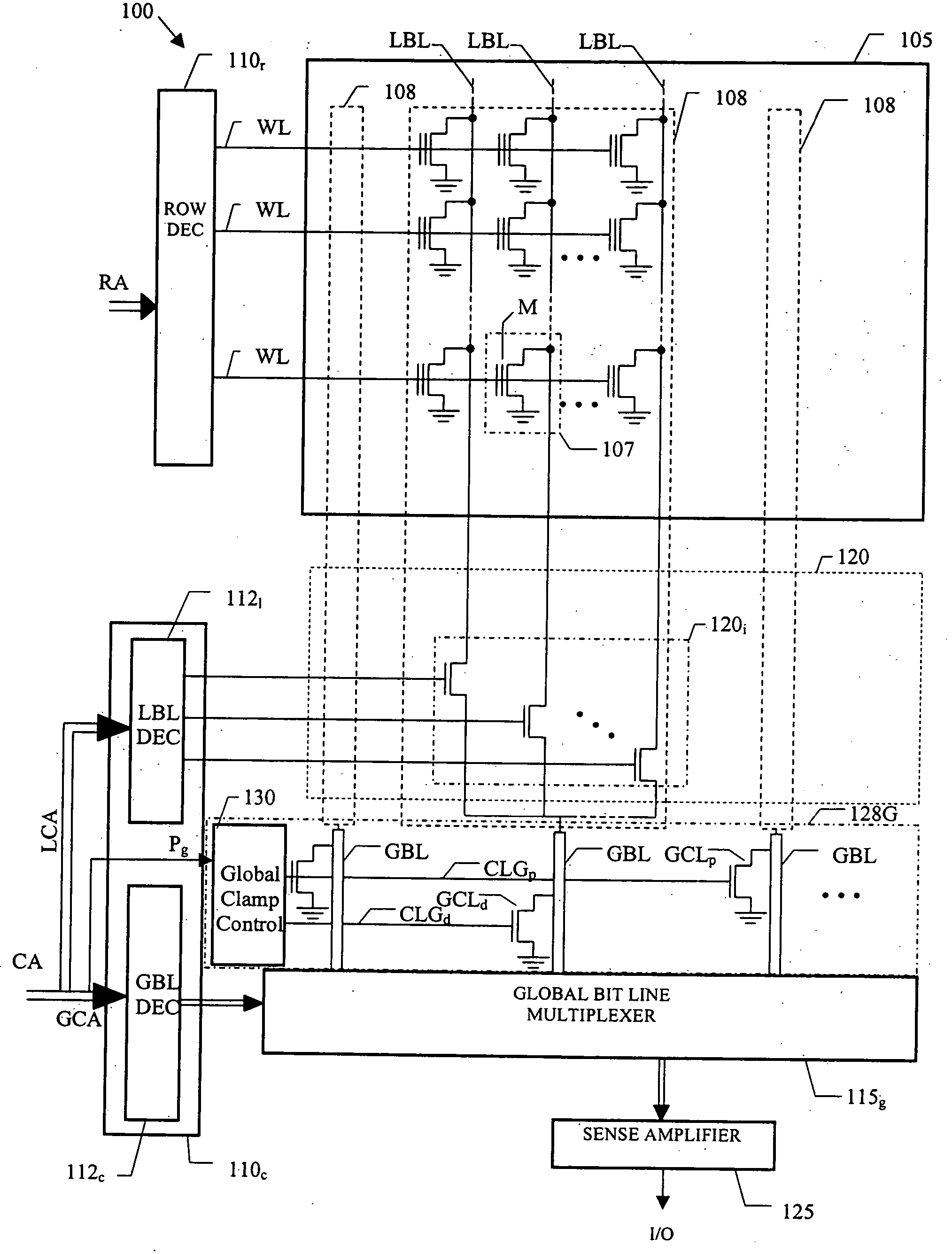
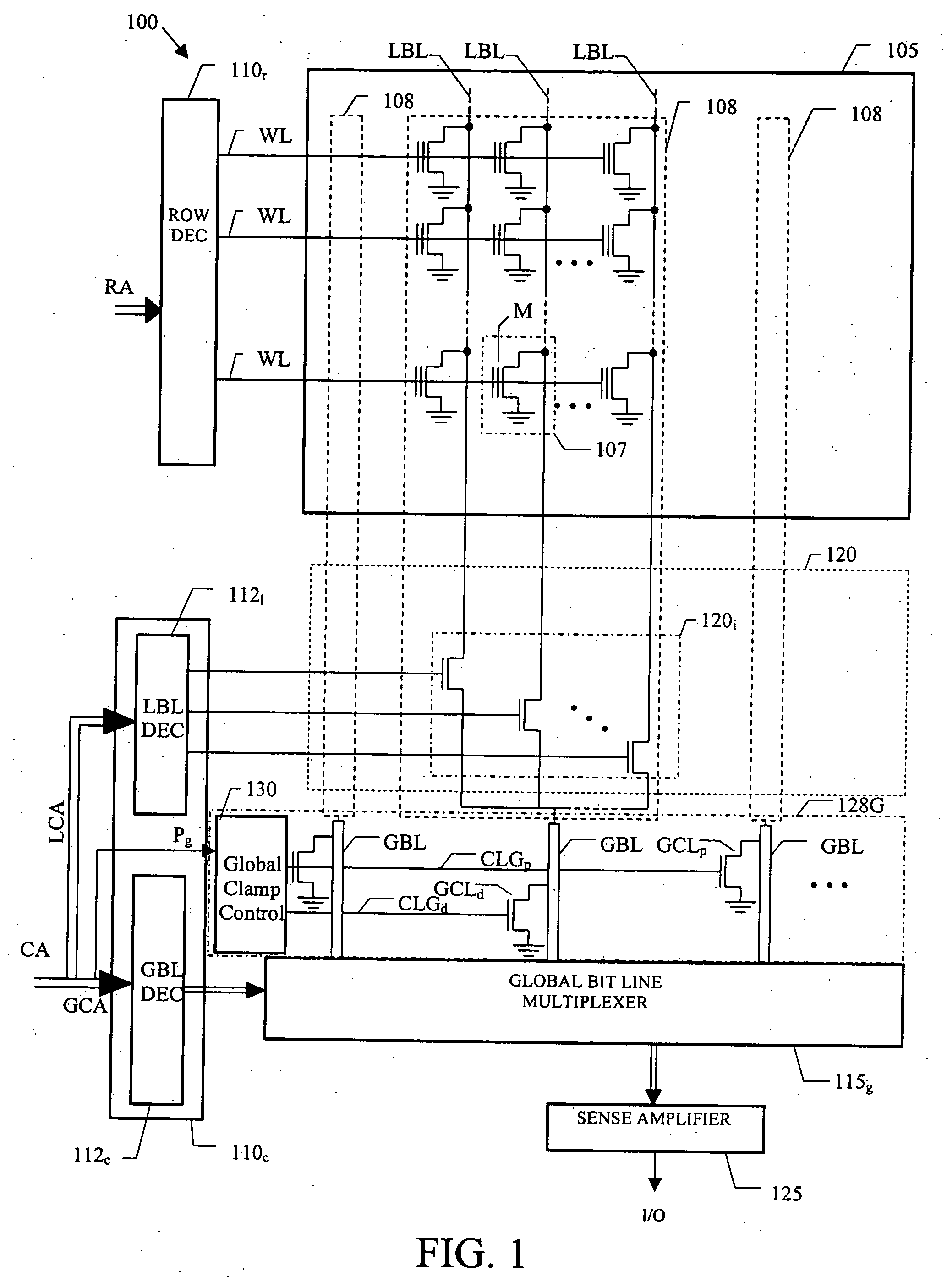
[0018] With reference to FIG. 1, a portion of a non-volatile memory device 100, in particularly a flash E2PROM, is schematically illustrated. The flash memory 100 is integrated in a chip of semiconductor material; a matrix 105 of memory cells 107 (particularly, a memory matrix having a NOR architecture, as shown in the FIG. 1) is used for storing data.

[0019] Each cell 107 includes a floating gate MOS transistor M. In an erased condition, the cell 107 has a low threshold voltage. The cell 107 is programmed by injecting electric charges into its floating gate; in the programmed condition, the memory cell 107 has a high threshold voltage value. Therefore, the value of the threshold voltage defines the different logic values that the datum stored in the memory cell 107 may assume. The memory cell is erased by removing the electrical charge stored in its floating gate.

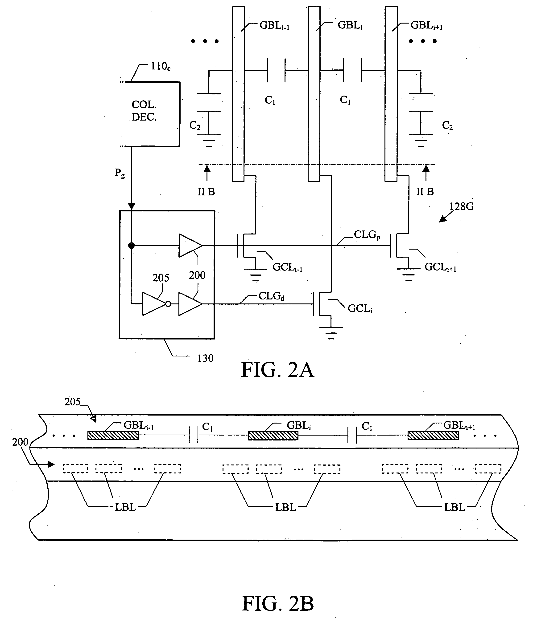
[0020] The memory cells 107 are organized by rows and columns. The matrix 105 includes a word line WL per each row. The...


PUM


Abstract

A semiconductor memory device is provided. The semiconductor memory device includes a memory matrix having a plurality of memory cells arranged according to a plurality of rows and a plurality of columns and a plurality of bit lines, each bit line being associated with at least one respective column of said plurality. The semiconductor memory device further includes a bit line selection structure for selecting at least one among said bit lines and a voltage clamping circuit structure adapted to cause the clamping at a prescribed voltage of unselected bit lines adjacent and capacitively coupled to a selected bit line during a read operation.

Description

BACKGROUND OF THE INVENTION [0001] 1. Field of the Invention [0002] The present invention relates to the data storage field in general; more specifically, the present invention relates to a semiconductor memory device, particularly albeit not limitatively to a non-volatile semiconductor memory. [0003] 2. Description of the Related Art [0004] Non-volatile memory devices are commonly used to store information which must be preserved also in absence of an electric power source that supply the memory device. A particular class of non-volatile memory devices is electrically programmable; for example, flash E2PROM belong to such class. Typically, a flash memory includes a matrix of memory cells, each consisting of a floating gate MOS transistor programmed by injecting an electric charge into its floating gate; on the contrary, the transistor is erased by removing the electric charge from its floating gate. The electric charge in the floating gate of the transistor modifies its threshold v...

Claims


Application Information

Patent Timeline
IPC IPC(8): G11C7/10
CPCG11C7/12G11C7/18G11C16/24G11C2207/002
Inventor SFORZIN, MARCOCONFALONIERI, EMANUELEDEL GATTO, NICOLAPOIDOMANI, CARLA GIUSEPPINA
Owner MICRON TECH INC
Why Eureka
Try Eureka